Multilayer capacitor and method of manufacturing same

Active Publication Date: 2010-07-29
TDK CORPARATION
View PDF6 Cites 74 Cited by
  • Summary
  • Abstract
  • Description
  • Claims
  • Application Information

AI Technical Summary

Benefits of technology

[0028]Preferably, a surface of the lead frame is plated with solder. In this case, the terminal electrode of the capacitor element body and the terminal connecting surface can easily be connected to each other by heat treatment after mounting the capacitor element body on the terminal connecting surface.
[0029]As in the f

Problems solved by technology

This makes it hard to see the state of solder fillets from the outsi

Method used


Image

  • Multilayer capacitor and method of manufacturing same
  • Multilayer capacitor and method of manufacturing same
  • Multilayer capacitor and method of manufacturing same

Examples


first embodiment

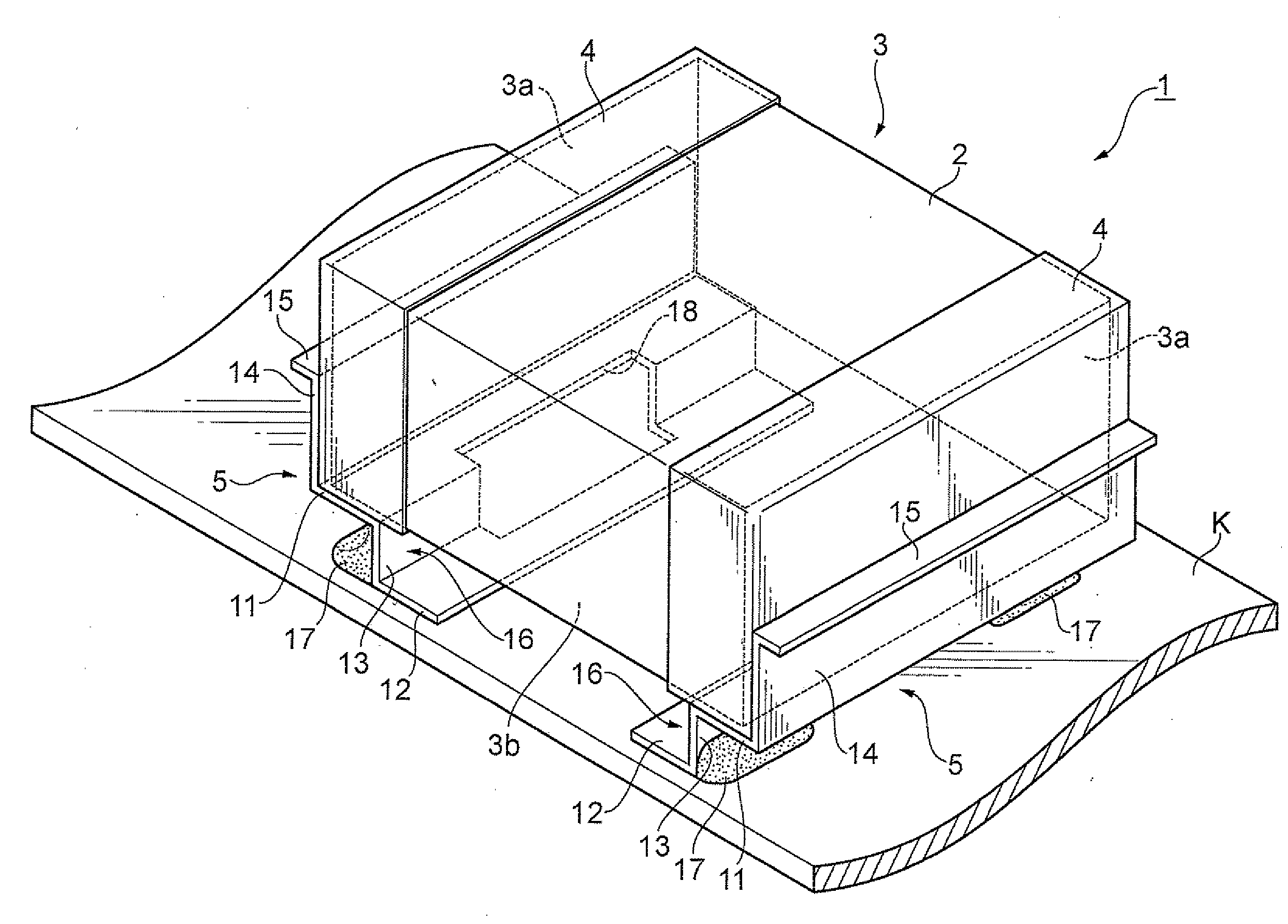
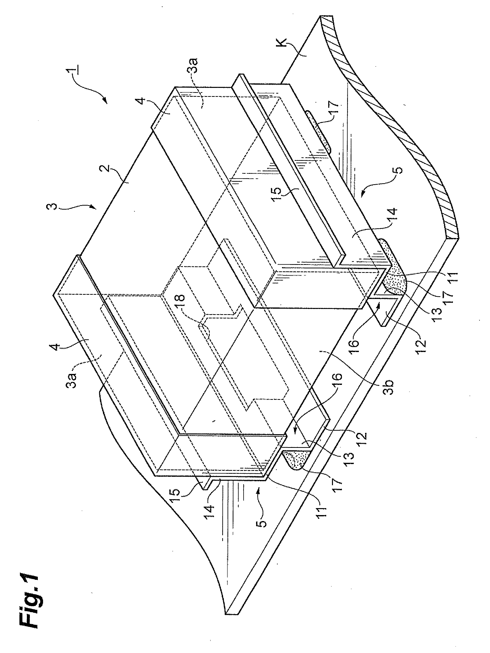
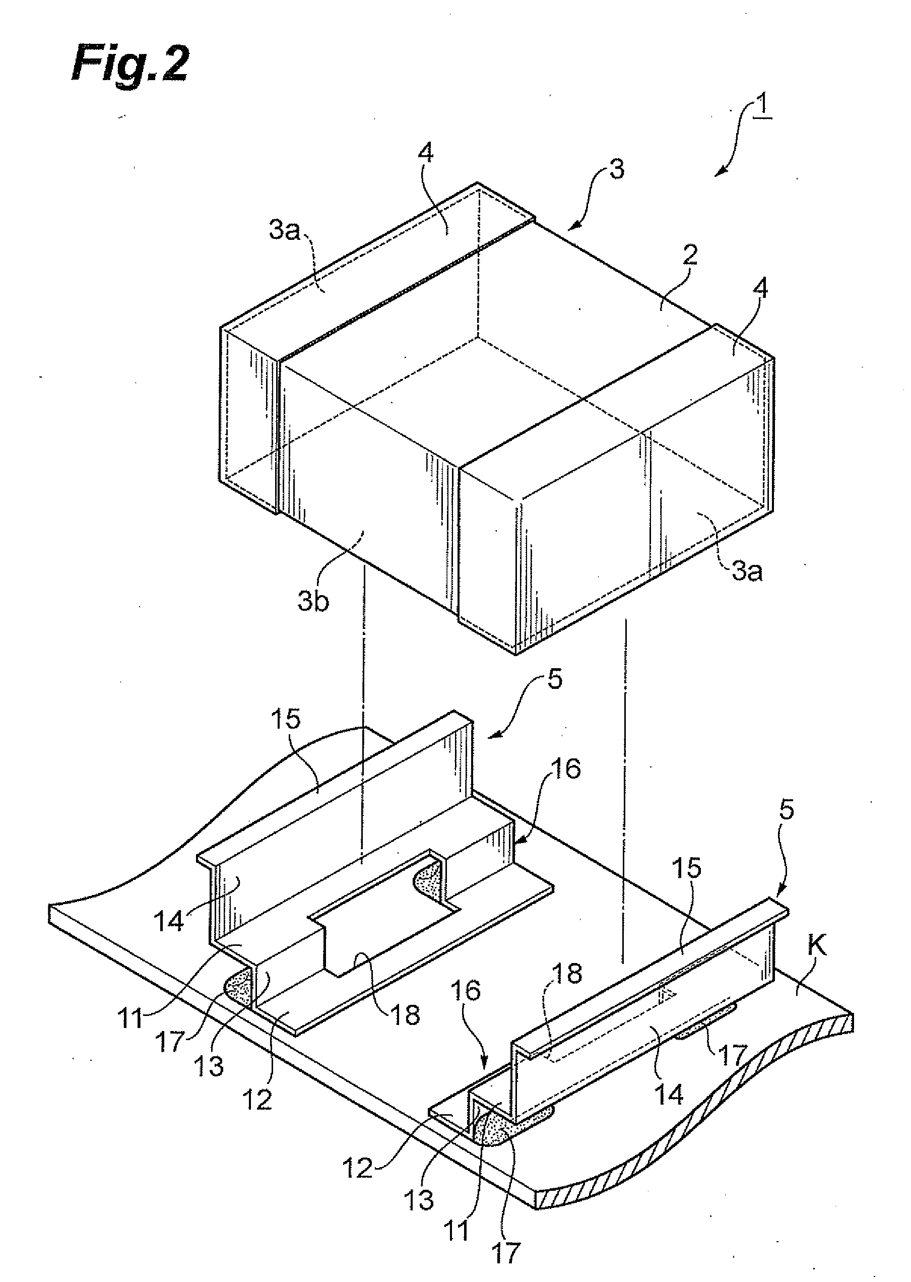
[0044]FIG. 1 is a perspective view illustrating the multilayer capacitor in accordance with the first embodiment of the present invention. FIG. 2 is an exploded perspective view of FIG. 1, while FIG. 3 is a side view thereof.

[0045]As illustrated in FIGS. 1 to 3, the multilayer capacitor 1 in accordance with the first embodiment, which is a multilayer ceramic capacitor of 2012 type (having a length of 2.0 mm, a width of 1.2 mm, and a height of 1.0 mm), for example, comprises a substantially rectangular parallelepiped capacitor element body 3 formed by laminating a plurality of dielectric layers 2, a pair of terminal electrodes 4, 4 formed so as to cover longitudinal end faces 3a, 3a of the capacitor element body 3, and a pair of metal terminals 5, 5 disposed about the capacitor element body 3.

[0046]The dielectric layers 2 constituting the capacitor element body 3 are formed by sintering a multilayer body of ceramic green sheets containing a dielectric ceramic based on BaTiO3, Ba(Ti, ...

second embodiment

[0068]The second embodiment of the present invention will now be explained. FIG. 6 is a perspective view illustrating the multilayer capacitor in accordance with the second embodiment of the present invention. FIG. 7 is an exploded perspective view of FIG. 6, while FIG. 8 is a side view thereof.

[0069]As illustrated in FIGS. 6 to 8, the multilayer capacitor 41 in accordance with the second embodiment differs from the first embodiment in the structure of a joint surface 53 in each metal terminal 45. That is, the joint surface 53 of the metal terminal 45 in the multilayer capacitor 41 is constituted by an intermediate surface 53a arranged at a position between the terminal connecting surface 51 and substrate connecting surface 52, a first rising surface 53b raised substantially at right angles from the substrate connecting surface 52 and joined to the intermediate surface 53a, and a second rising surface 53c raised substantially at right angles from the intermediate surface 53a and joi...


PUM

PropertyMeasurementUnit
Densityaaaaaaaaaa
Flexibilityaaaaaaaaaa
Areaaaaaaaaaaa

Abstract

A multilayer capacitor which can prevent chattering noises from occurring and improve the packaging density and packaging yield, and a method of manufacturing a multilayer capacitor are provided.
Even when an electrostrictive vibration is generated in this multilayer capacitor upon voltage application, a joint surface of a metal terminal can flex, so as to mitigate the electrostrictive vibration, thereby preventing chattering noises from occurring. The joint surface is formed with a cutout and thus can fully secure its flexibility. In this multilayer capacitor, a step formed by a terminal connecting surface, a substrate connecting surface, and the joint surface is positioned within an area overlapping a capacitor element body as seen in the laminating direction of dielectric layers. Therefore, solder fillets do not protrude out of the capacitor element body, whereby the packaging density on a mounting substrate K can be improved. The state of solder fillets is easy to see from the outside, and a connection yield can also be secured.

Description

BACKGROUND OF THE INVENTION[0001]1. Field of the Invention[0002]The present invention relates to a multilayer capacitor and a method of manufacturing the same.[0003]2. Related Background Art[0004]A multilayer capacitor comprising a capacitor element body formed by laminating a plurality of dielectric layers, a plurality of inner electrodes formed within the capacitor element body, and a pair of terminal electrodes formed on side faces of the capacitor element body has conventionally been known. When a voltage is applied to the multilayer capacitor, a mechanical strain having a magnitude corresponding to the applied voltage is generated in the capacitor element body because of the electrostrictive effect. When an AC voltage is applied, the mechanical strain causes vibrations (electrostrictive vibrations) in the multilayer capacitor in particular. Hence, when an AC voltage is applied to a multilayer capacitor mounted on a substrate, electrostrictive vibrations may propagate to the sub...

Claims


Application Information

Patent Timeline
IPC IPC(8): H01G4/228H01L21/00
CPCH01G2/06H01G4/232H01G4/30Y10T29/41H05K2201/10636H05K2201/10856H05K2201/10946H05K3/3426Y02P70/50
Inventor TOGASHI, MASAAKIMASUDA, SUNAOABE, HIROSHI
Owner TDK CORPARATION
Why Eureka
Try Eureka