Semiconductor chip package

a semiconductor chip and chip package technology, applied in the field of semiconductor chip packaging, can solve the problems of reducing resistance and reducing the length of leads, and achieve the effects of reducing the area and height of the semiconductor chip package, reducing the length of leads, and reducing electrical and thermal resistan

Inactive Publication Date: 2010-08-05
ZETEX SEMICON PLC
View PDF18 Cites 12 Cited by
  • Summary
  • Abstract
  • Description
  • Claims
  • Application Information

AI Technical Summary

Benefits of technology

[0015]Advantageously, the present invention provides a reliable semiconductor device package having a lead frame construction, which results in a very low electrical and thermal resistance. By reducing the thickness of parts of the leads and bending the leads the area and height of the semiconductor chip package can be reduced. Furthermore, the length of the leads is reduced, reducing the resistance of the lead. The partially thinned and bent leads also serve to reduce the incidence of the encapsulating material delaminating from the lead frame. The lead frame is readily adaptable to accommodate different chip thicknesses, without significant redesign of the lead frame.

Problems solved by technology

Furthermore, the length of the leads is reduced, reducing the resistance of the lead.

Method used


Image

  • Semiconductor chip package
  • Semiconductor chip package
  • Semiconductor chip package

Examples


Embodiment Construction

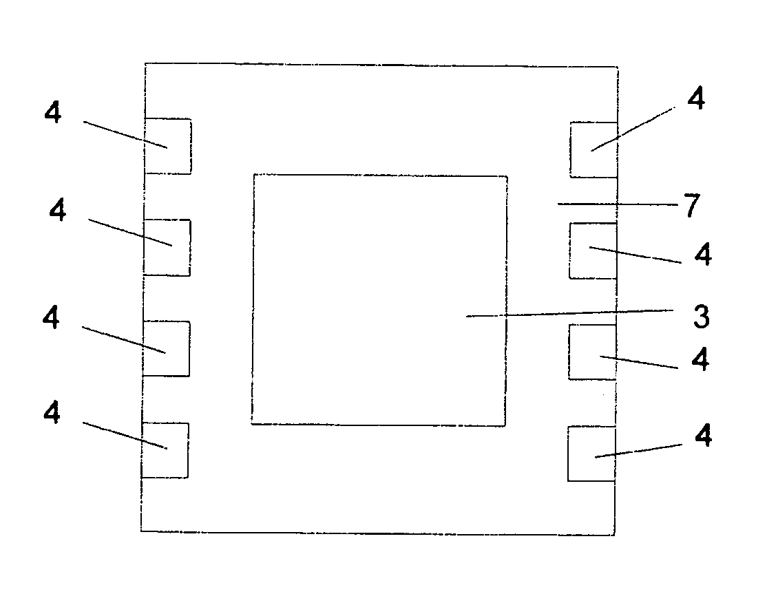
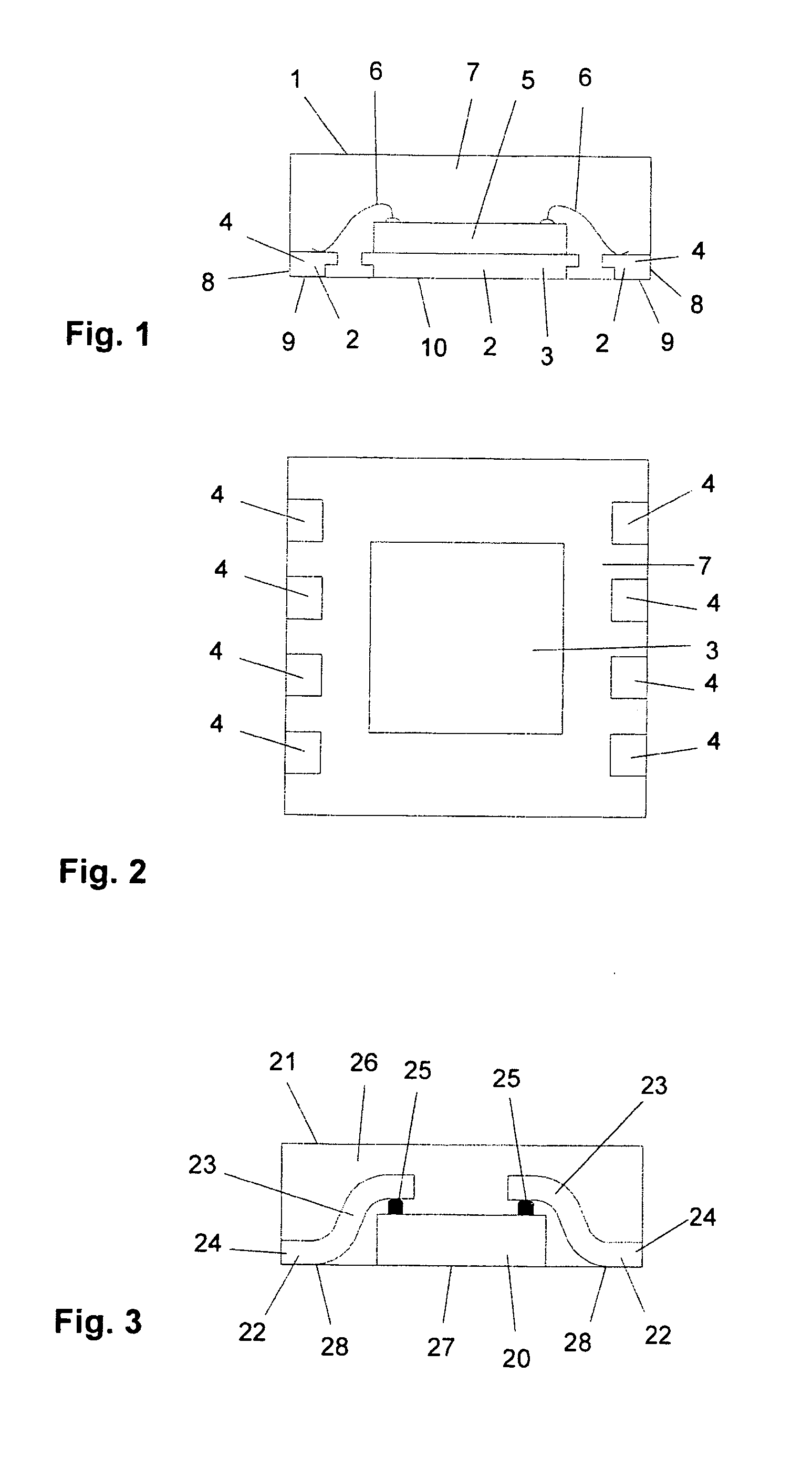
[0053]Referring first to FIG. 1, this schematically illustrates, in cross section, a known form of surface mounted leadless semiconductor chip package 1. The chip package 1 comprises a lead frame 2, comprising a chip pad 3 and lead pads 4. A semiconductor chip 5 is attached to the chip pad 3 by an adhesive compound. Surface portions of the semiconductor chip 5 are connected to the lead pads 4 via wire bonds 6. The lead frame 2, chip 5 and wire bonds 6 are encapsulated by a resin layer 7. The term resin layer, as used throughout the description, is intended to refer to any material that partially or fully encapsulates the semiconductor chip and other components. The term is not intended to be restricted to any particular material. Side 8 and base 9 portions of the lead pads 4 and the base 10 of the chip pad 3 are exposed at the exterior of the semiconductor chip package 1 for electrical connection (i.e. the resin layer 7 does not fully surround the chip package 1). The exposed chip p...


PUM


Abstract

A semiconductor chip package is disclosed comprising a semiconductor chip, a lead frame comprising at least one lead, and an encapsulating layer at least partially encapsulating the semiconductor chip and the lead frame. The lead comprises a first portion defining a lead frame pad at least partially exposed at an exterior surface of the package and a second portion extending from the first portion towards the semiconductor chip electrically connecting a surface portion of the semiconductor chip to the lead frame pad. The first portion has a first thickness and the second portion comprises a thinned portion, the thinned portion having a thickness smaller than the first thickness. The lead further comprises a bent portion, and wherein the thinned portion comprises at least part of the bent portion.

Description

FIELD OF THE INVENTION[0001]The present invention relates to packaging of semiconductor chips. In particular, but not exclusively, the present invention relates to semiconductor chips having a moulded package and specifically leadless surface mounted semiconductor chip packages. A method of fabricating such a semiconductor chip package is also provided.BACKGROUND OF THE INVENTION[0002]There is an increasing requirement for semiconductor chip packages having compact structures in order to minimise the space required within consumer appliances. Furthermore, specialist applications, such as mobile telephones, require lightweight, space efficient packaging structures. While there has been a significant reduction in the size and weight of semiconductor chip packages in recent years, there is still a need for further improvements.[0003]There are a large number of known semiconductor chip packaging technologies. Both ceramic and plastic materials have been used to encapsulate, and thereby ...

Claims


Application Information

Patent Timeline
Patent Type & Authority Applications(United States)
IPC IPC(8): H01L23/495H01L23/488H01L21/60H01L21/56
CPCH01L23/3107H01L2924/1305H01L23/49551H01L23/49562H01L23/49568H01L23/49575H01L24/36H01L24/40H01L24/41H01L2224/48091H01L2224/48247H01L2924/01013H01L2924/01027H01L2924/01029H01L2924/01033H01L2924/01079H01L2924/01082H01L2924/04953H01L2924/14H01L2924/30105H01L2924/30107H01L23/49548H01L2224/16245H01L2924/3011H01L2924/01047H01L2924/01006H01L24/48H01L2924/00014H01L2924/00H01L2224/40137H01L2924/181H01L2924/18161H01L2224/84801H01L2224/37147H01L2224/8385H01L2224/3716H01L2224/37155H01L2224/3754H01L24/37H01L2224/371H01L24/84H01L2924/00012H01L2224/45099H01L2224/45015H01L2924/207H01L2224/73221H01L21/4821
Inventor KASTNER, RAINERDOBERSCHUTZ, FRANK-MICHAEL
Owner ZETEX SEMICON PLC
Why Eureka
Try Eureka