Chip antenna

a chip antenna and chip technology, applied in the direction of antennas, antenna details, electrically short antennas, etc., can solve the problems of limited chip antenna bandwidth, limited micro-strip length, and limited chip antenna area, so as to increase the area for transmitting and increase the bandwidth of chip antennas

Inactive Publication Date: 2010-08-12
CHANG SIN MIN
View PDF3 Cites 0 Cited by
  • Summary
  • Abstract
  • Description
  • Claims
  • Application Information

AI Technical Summary

Benefits of technology

[0009]A main object of the present invention is to provide a chip antenna which can increase the area for transmitti

Problems solved by technology

Chip antennas have the advantage of small volume; however, small volume also limits the length of the micro strips, so that the radiation areas of chip antennas are obviously smaller than those of conventional antennas.
Therefore

Method used


Image

  • Chip antenna
  • Chip antenna
  • Chip antenna

Examples


Embodiment Construction

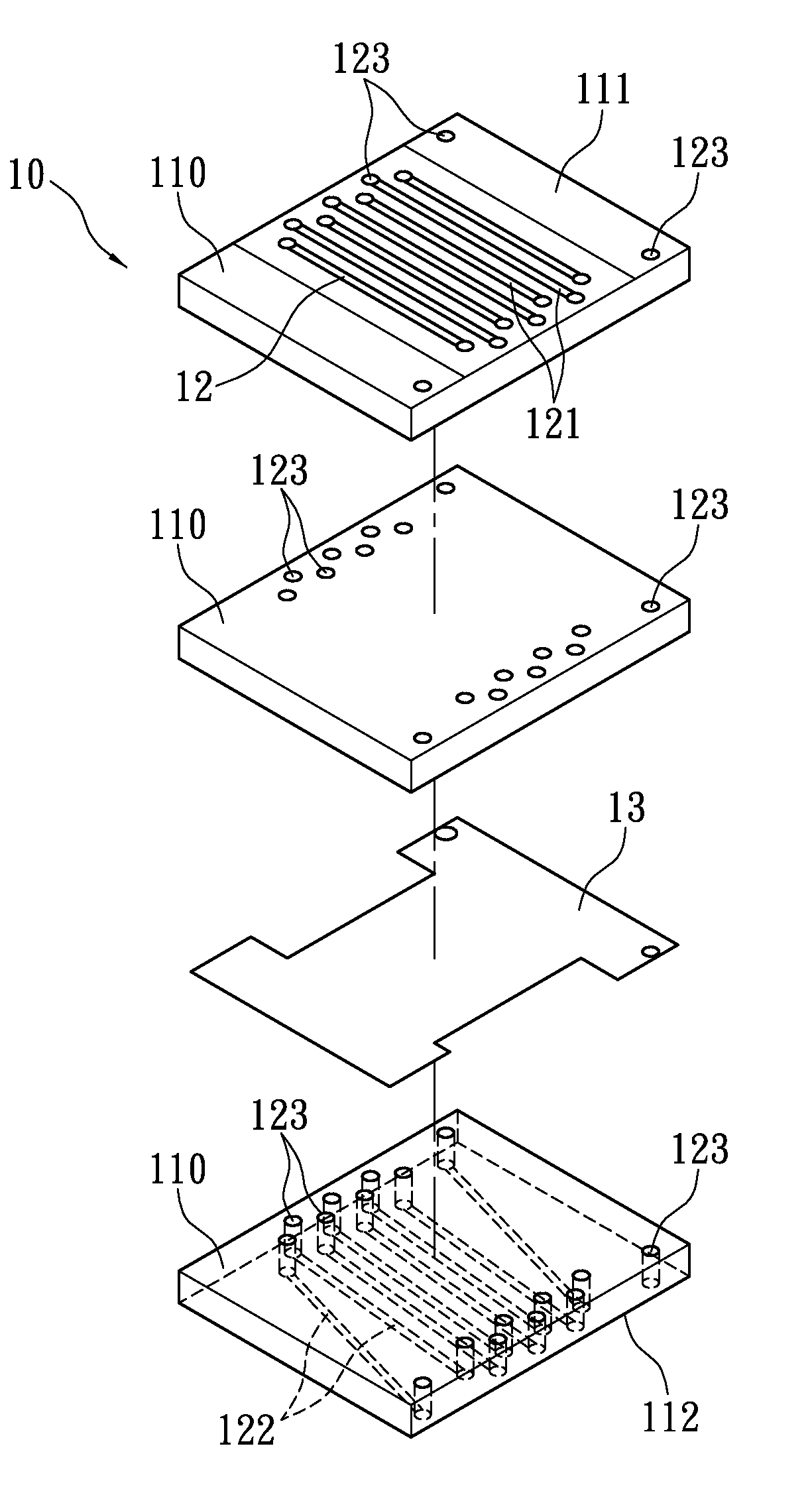
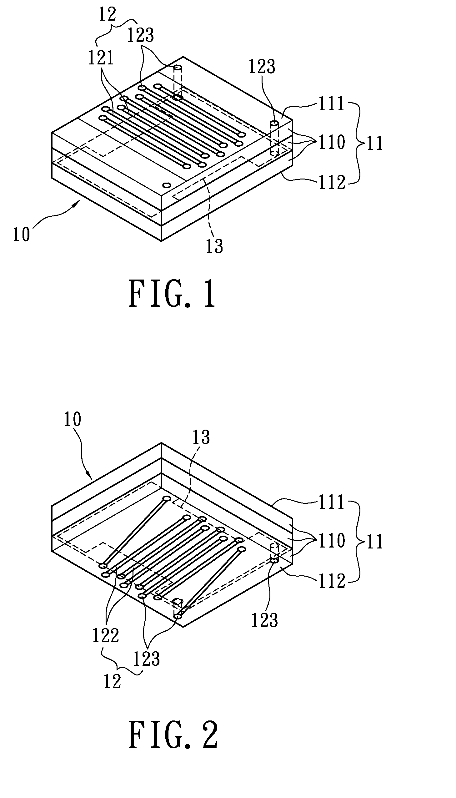
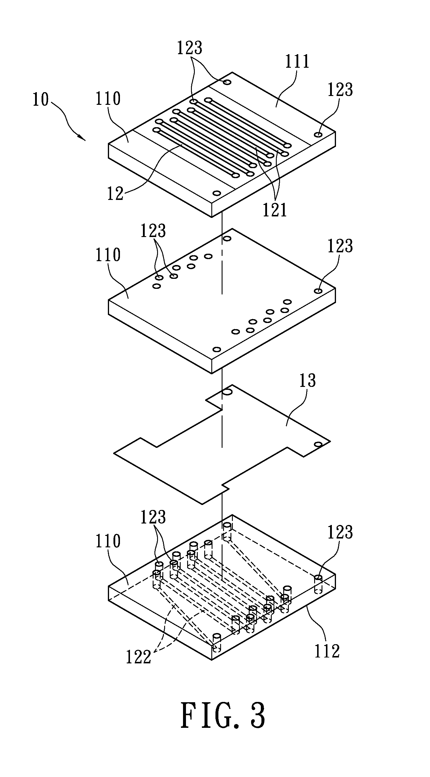
[0021]Please refer to FIGS. 1-3 illustrating a chip antenna 10 according to the present invention. The chip antenna 10 includes a main body 11, a microstrip structure 12, and a metal piece 13.

[0022]The main body 11 is formed by overlapping three first circuit boards 110. The main body 11 has a length of 5.4 mm, a width of 4.5 mm, and a thickness of 1.6 mm, wherein the two upper first circuit boards 110 have a thickness of 0.4 mm, and the lowest first circuit board 110 has a thickness of 0.8 mm. The material of the first circuit boards 110 may be Flame Retardant 4 (FR-4) and so on.

[0023]For the following description, the upper surface of the main body 11 is defined as a first surface 111 and the lower surface thereof is defined as a second surface 112. The microstrip structure 12 is disposed on the first surface 111 and the second surface 112. The metal piece 13 is disposed in the main body 11 and clamped between two of the first circuit boards 110. The area of the metal piece 13 is ...


PUM


Abstract

A chip antenna includes a main body having a first surface and a second surface; a microstrip structure disposed on the first surface and the second surface of the main body; and at least one metal piece which is disposed in the main body and located between the first surface and the second surface, the metal piece is electrically connected with the microstrip structure. Since the area of the metal piece is almost equal to that of the first surface or the second surface of the main body, therefore the metal piece can increase the radiation area of the chip antenna greatly so that the chip antenna have greater bandwidth and better electrical characteristics.

Description

BACKGROUND OF THE INVENTION[0001]1. Field of the Invention[0002]The present invention relates to a chip antenna, and more specifically to a chip antenna with a metal piece.[0003]2. Description of Related Art[0004]With the rapid development of wireless communication industry, most of the electronic products (for example, mobile phones, personal digital assistants, notebook computers, sensing equipments, etc.) transmit signals via wireless communication. Antennas disposed on electronic products act as one primary type of equipment for transmitting and receiving signals in wireless communication. Therefore the popularity and needs for antennas are constantly increasing.[0005]For reducing manufacture costs of antennas and meeting design requirements that the electronic products must be smaller, lighter, and thinner, most of the electronic wireless communication products replace conventional antennas that has large volume (for example, rod antenna) with chip antennas with smaller volume....

Claims


Application Information

Patent Timeline
IPC IPC(8): H01Q1/38
CPCH01Q1/2283
Inventor CHANG, SIN-MIN
Owner CHANG SIN MIN
Why Eureka
Try Eureka