Semiconductor memory device, memory module including the same, and data processing system

Inactive Publication Date: 2010-08-19
PS4 LUXCO SARL
View PDF5 Cites 65 Cited by
  • Summary
  • Abstract
  • Description
  • Claims
  • Application Information

AI Technical Summary

Benefits of technology

[0016]According to the semiconductor device of the present invention, when the device enters the write leveling mode, a counter that counts latency of the ODT signal is bypassed. Therefore, when the ODT signal is input, the terminating resistance circuit can be immediately activated asynchronously with a clock. Accordingly, the semiconductor device can quickly perform a write leveling operation without waiting for the latency of the ODT signal. Furthermore, because the terminating resistance circuit is not activated constantly but

Problems solved by technology

However, the write data fetched by the semiconductor memory device is transferred to a memory cell array synchronously with a clock signal, which is different from the data strobe signal.
Therefore, when a skew exists between the data strobe signal and the clock signal, a write operation cannot be performed correctly.
Consequently, the write leve

Method used


Image

  • Semiconductor memory device, memory module including the same, and data processing system
  • Semiconductor memory device, memory module including the same, and data processing system
  • Semiconductor memory device, memory module including the same, and data processing system

Examples


Example

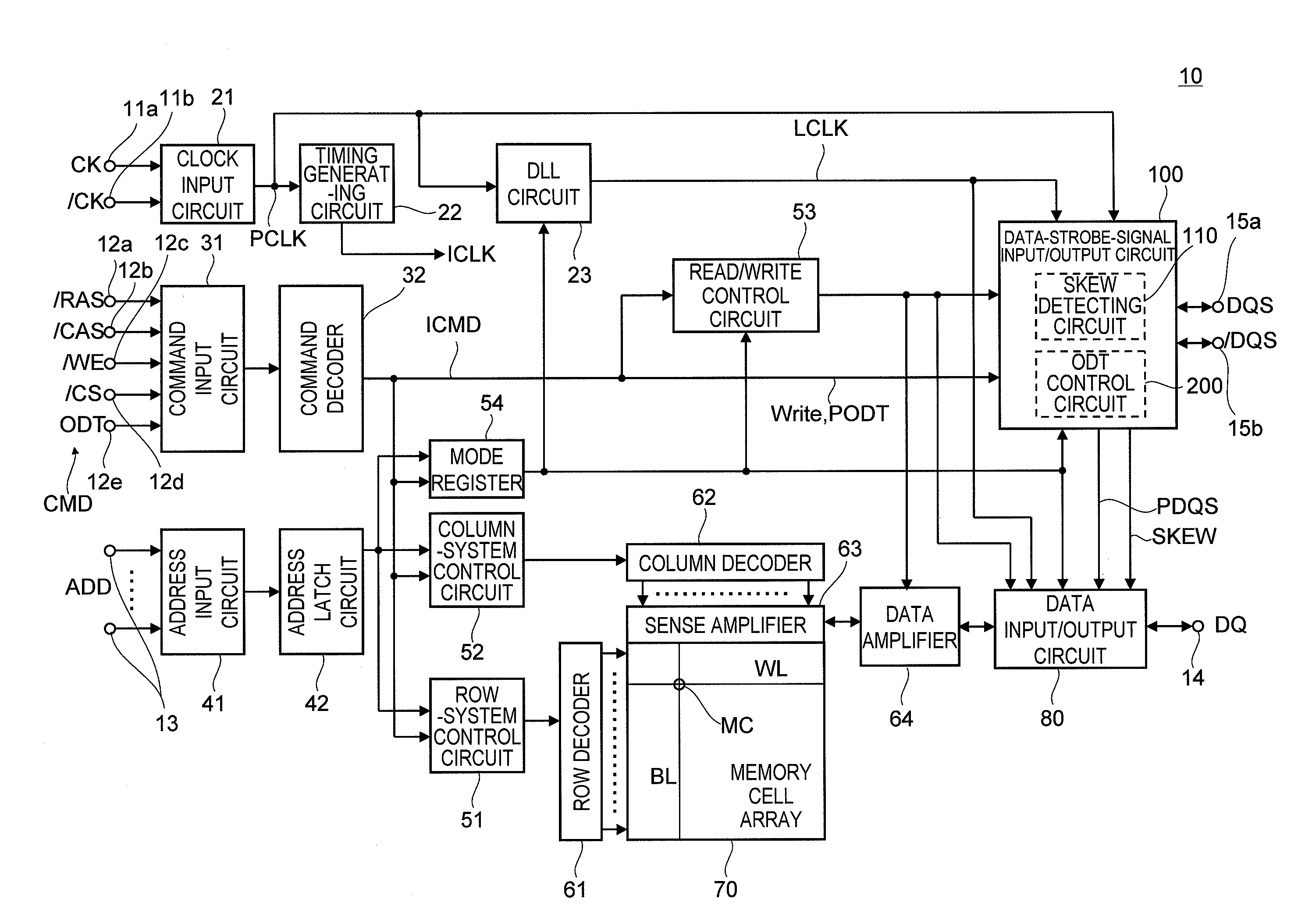
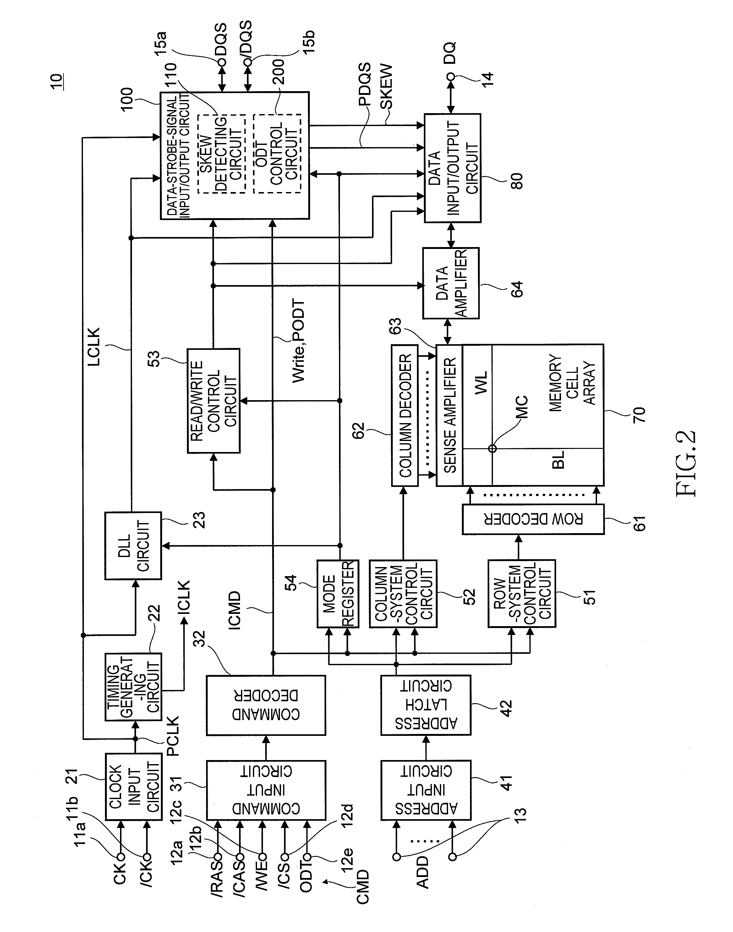
[0027]Preferred embodiments of the present invention will be explained below in detail with reference to the accompanying drawings.

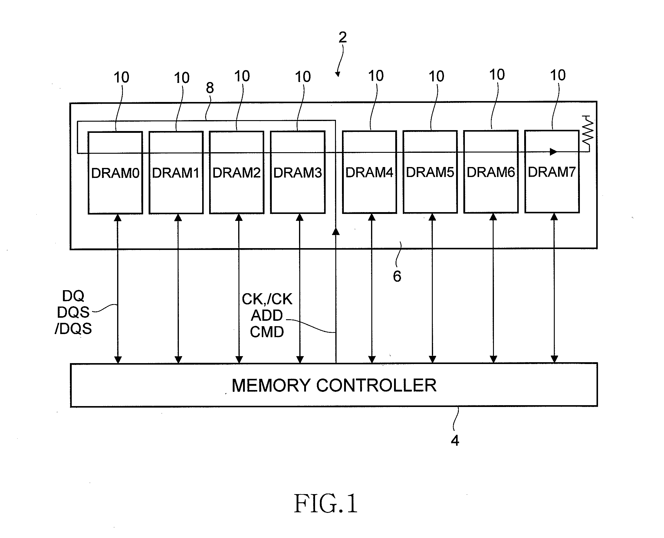
[0028]FIG. 1 shows a configuration of a data processing system according to a preferred embodiment of the present invention.

[0029]The data processing system shown in FIG. 1 includes a memory module 2 and a memory controller 4 connected to the memory module 2. The memory module 2 has plural semiconductor memory devices 10 (DRAM0 to DRAM7) mounted on a module substrate 6. While the memory module 2 shown in FIG. 1 has eight DRAMs of DRAM0 to DRAM7 on the module substrate 6, the number of the semiconductor memory devices 10 mounted on the module substrate 6 is not limited thereto. The semiconductor memory devices 10 can be mounted on either one side or both sides of the module substrate 6. The structure and material of the module substrate 6 are not particularly limited.

[0030]The type of the semiconductor memory devices 10 is not also particularly limited. I...


PUM


Abstract

To provide a semiconductor device including a skew detecting circuit activated in a write leveling mode, and an ODT control circuit that activates a terminating resistance circuit connected to a data strobe terminal by using an ODT signal. The ODT control circuit includes counters that delay the ODT signal, activates the terminating resistance circuit by using the ODT signal having passed the counters in a normal operation mode, and activates the terminating resistance circuit by using the ODT signal having bypassed the counters in the write leveling mode. With this configuration, in the write leveling mode, a write leveling operation can be performed quickly without waiting for latency of the ODT signal.

Description

BACKGROUND OF THE INVENTION[0001]1. Field of the Invention[0002]The present invention relates to a semiconductor device, and more particularly relates to a semiconductor device having a write leveling mode for measuring a skew between a clock signal and a data strobe signal. The present invention also relates to a module including this semiconductor device and to a data processing system.[0003]2. Description of Related Art[0004]Transmission and reception of read data and write data between a semiconductor memory device such as a DRAM (Dynamic Random Access Memory) and a memory controller may be performed synchronously with a data strobe signal. For example, in a write operation, a memory controller supplies a data strobe signal and write data to a semiconductor memory device, and the semiconductor memory device fetches the write data synchronously with the data strobe signal.[0005]However, the write data fetched by the semiconductor memory device is transferred to a memory cell arra...

Claims


Application Information

Patent Timeline
IPC IPC(8): G11C7/00G11C8/18H03K19/003
CPCG11C7/1066G11C7/1078G11C7/1084G11C11/4093G11C7/222G11C11/4076G11C7/22
Inventor FUJISAWA, HIROKI
Owner PS4 LUXCO SARL
Why Eureka
Try Eureka