Clock buffer

Active Publication Date: 2010-08-26
TEXAS INSTR INC
View PDF11 Cites 6 Cited by
  • Summary
  • Abstract
  • Description
  • Claims
  • Application Information

AI Technical Summary

Benefits of technology

[0006]A preferred embodiment of the present invention, accordingly, provides an apparatus. The apparatus comprises a first bipolar junction transistor (BJT) differential pair having a first BJT and a second BJT; a second BJT differential pair having a third BJT and a fourth BJT, wherein the collector and base of the third BJT are respectively coupled to the collector and base of the first BJT, and wherein the collector and base of the of the fourth BJT are respectively coupled to the collector and base of the second BJT, and wherein the bases of first, second, third, and fourth BJTs receive an input clock signal; a first clamp having a fifth BJT and a sixth BJT, wherein the emitters of the fifth and sixth BJTs are coupled to the

Problems solved by technology

Typically, these clock input buffers have a relatively high gain and drive relatively high capacitance loads, and these clock input buffers, oftentimes, have to contend with difficult situations, such as jitter.
Application of the narrow bandpass filter, though, typically results in a sine wave-like input (i.e., slow edge rates) to the clock input buffers.
This combination of high gain and ability to drive a load capacitance results in a circuit that consumes high power.
As a result of this configuration, the current is generally high enough to have a very high slew rate, causing higher power consumption especially when the inputs are not toggling.

Method used


Image

  • Clock buffer
  • Clock buffer
  • Clock buffer

Examples


Embodiment Construction

[0019]Refer now to the drawings wherein depicted elements are, for the sake of clarity, not necessarily shown to scale and wherein like or similar elements are designated by the same reference numeral through the several views.

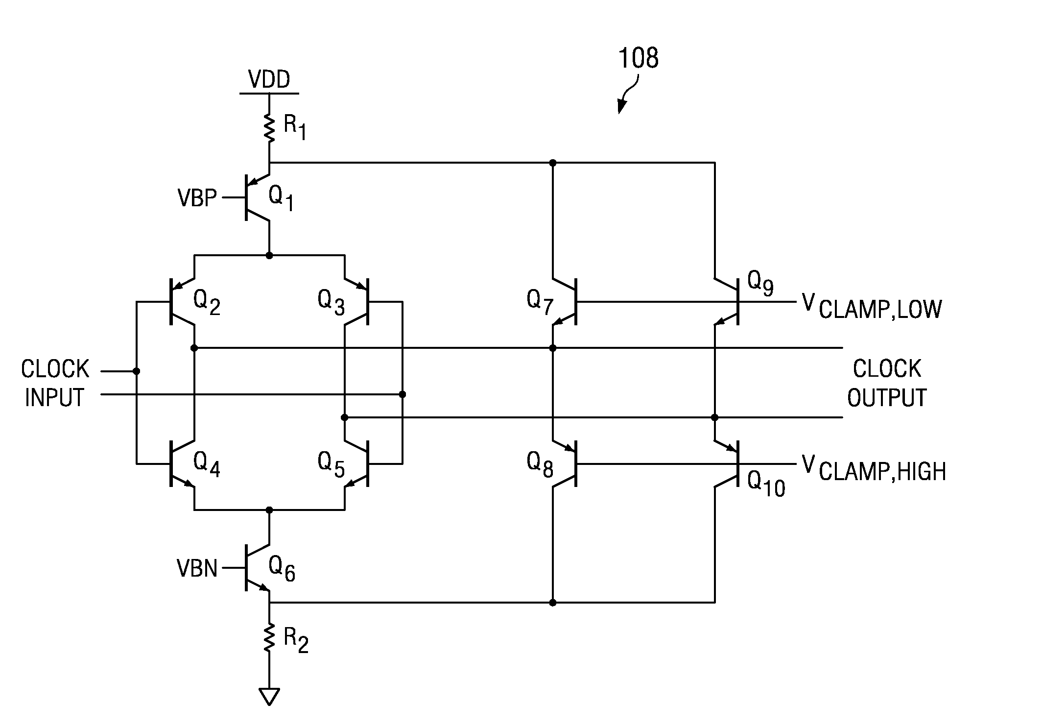
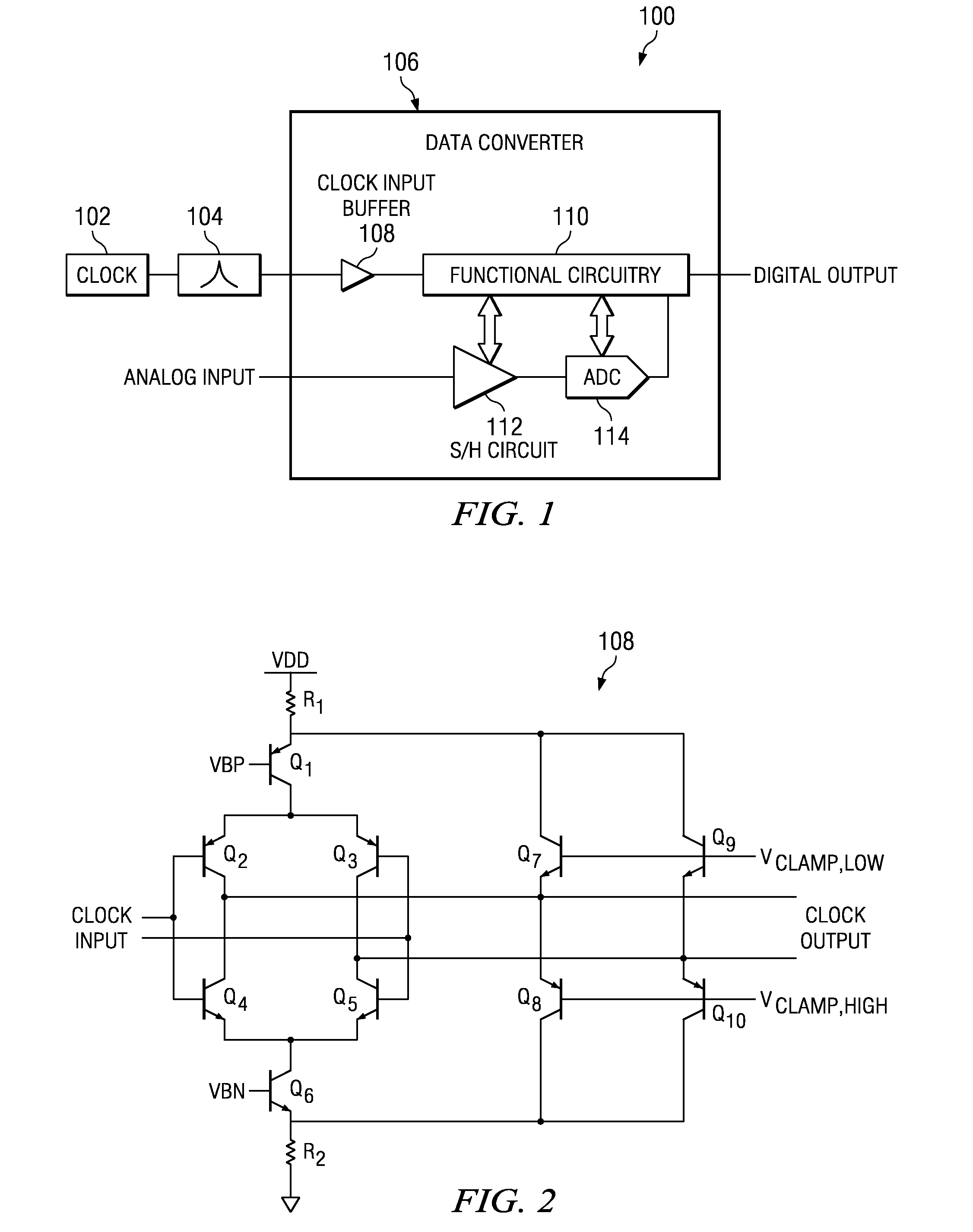
[0020]Referring to FIG. 1 of the drawings, the reference numeral 100 generally designates a system in accordance with a preferred embodiment of the present invention. The system 100 generally comprises a clock or oscillator 100, a narrowband filter 104, and a data converter 106. Moreover, the data converter 106 generally comprises a clock input buffer 108, functional circuitry 110, a sample-and-hold (S / H) circuit 112, and an analog-to-digital converter (ADC) 114.

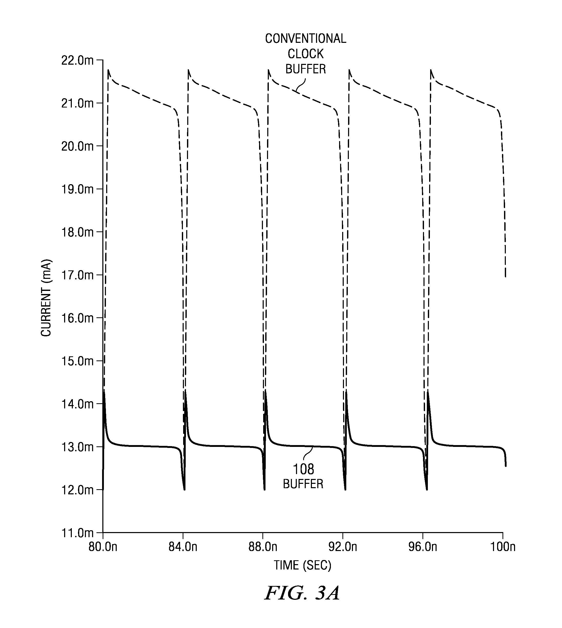
[0021]In operation, the data converter 106 is able to receive an analog input signal and convert it to a digital input signal across several channels. Clock 102 is able to generate a signal (which is generally in the 100 MHz to 200 MHz range). Because of the high frequency range of the analog input sig...


PUM


Abstract

An apparatus is provided. The apparatus comprises a first bipolar junction transistor (BJT) differential pair having a first BJT and a second BJT, a second BJT differential pair having a third BJT and a fourth BJT, a first clamp having a fifth BJT and a sixth BJT, and a second clamp having a seventh BJT and an eighth BJT. The collector and base of the third BJT are respectively coupled to the collector and base of the first BJT, and the collector and base of the fourth BJT are respectively coupled to the collector and base of the second BJT. The bases of first, second, third, and fourth BJTs receive an input clock signal. The emitters of the fifth and sixth BJTs are coupled to the collectors of the first and third BJTs, while the emitters of the seventh and eight BJTs are coupled to the collectors of the second and fourth BJTs. The bases of the fifth and seventh BJT are adapted to receive a low clamping voltage, and the bases of the sixth and eighth BJTs are adapted to receive a high clamping voltage. Additionally, the first and second clamps is coupled to the collectors of the first, second, third, and fourth BJTs.

Description

TECHNICAL FIELD[0001]The invention relates generally to a clock buffer and, more particularly, to clock buffer for an analog-to-digital converter (ADC).BACKGROUND[0002]Clock input buffers are used in a number of applications today. Typically, these clock input buffers have a relatively high gain and drive relatively high capacitance loads, and these clock input buffers, oftentimes, have to contend with difficult situations, such as jitter. Particularly, with many high performance applications (e.g., analog-to-digital converters or ADCs), the signal-to-noise ratio or SNR at very high input frequencies is dominated by clock jitter. For these applications, the clock input to the device can be externally filtered by an extremely narrow bandpass filter that effectively reduces the clock jitter. Application of the narrow bandpass filter, though, typically results in a sine wave-like input (i.e., slow edge rates) to the clock input buffers. To compensate for these sine wave-like inputs, th...

Claims


Application Information

Patent Timeline
IPC IPC(8): H03B1/00
CPCH03M1/1245H03M1/002
Inventor PAYNE, ROBERT F.CORSI, MARCOHSIEH, TIEN-LING
Owner TEXAS INSTR INC
Why Eureka
Try Eureka