Display device and method of manufacturing same

Active Publication Date: 2010-08-26
JAPAN DISPLAY INC
View PDF5 Cites 131 Cited by
  • Summary
  • Abstract
  • Description
  • Claims
  • Application Information

AI Technical Summary

Benefits of technology

[0030]According to the present embodiments, a method of manufacturing a display device which method does not incre

Problems solved by technology

A substrate where transparent electrodes are disposed to cancel the pattern of the transparent electrodes in the large

Method used


Image

  • Display device and method of manufacturing same
  • Display device and method of manufacturing same
  • Display device and method of manufacturing same

Examples


first embodiment

1. First Embodiment

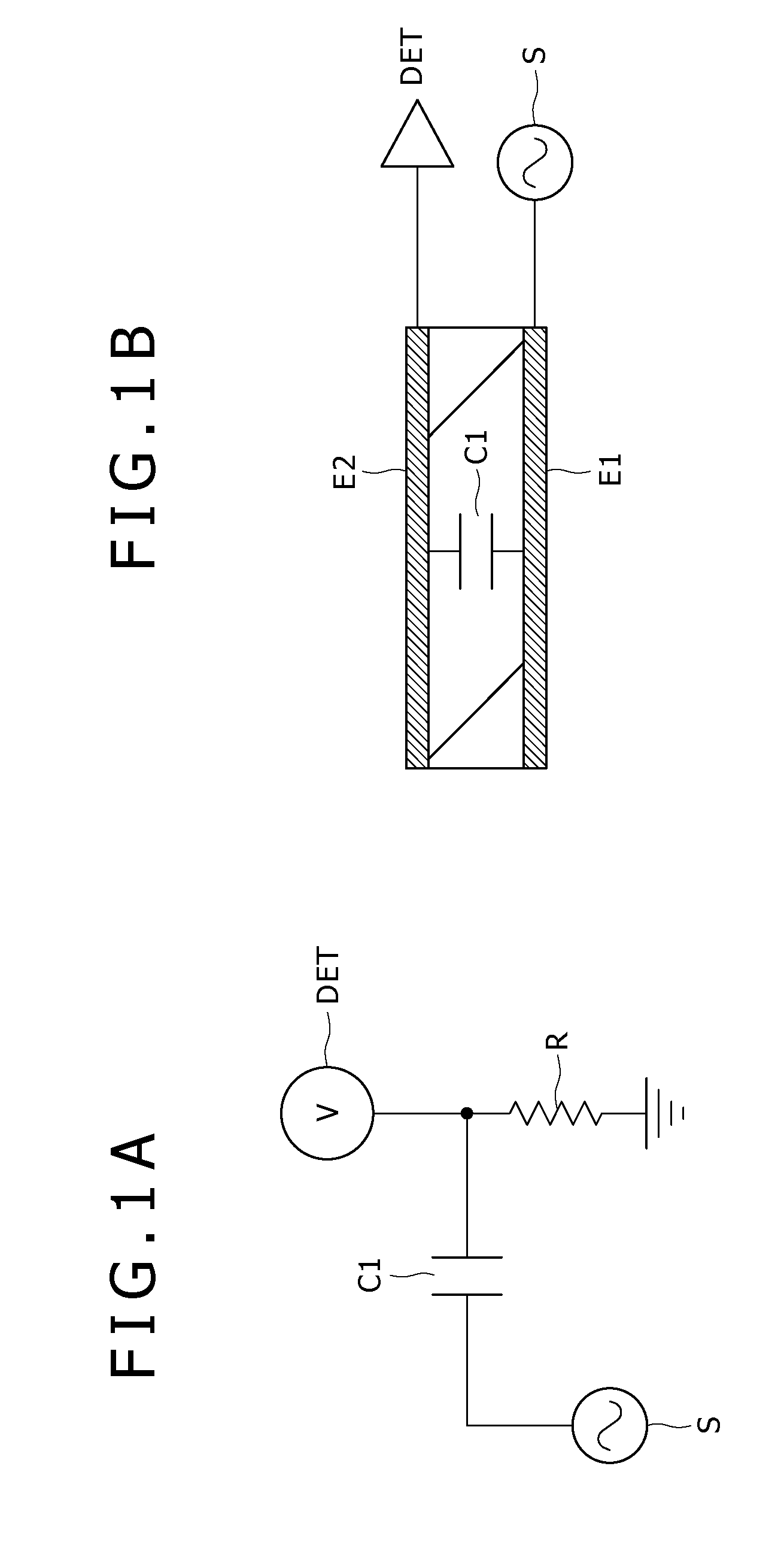
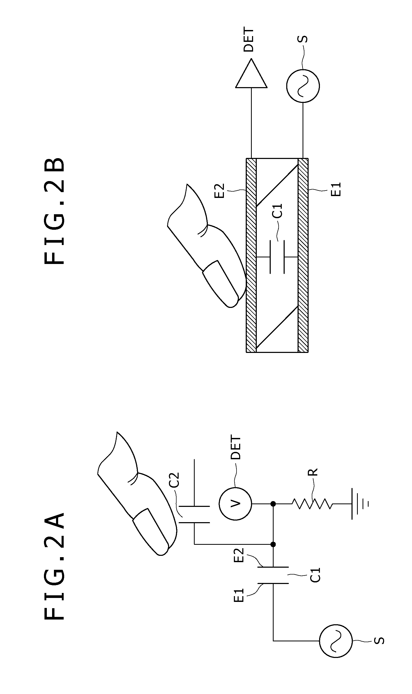
[0051]An electrode that is provided farther into a panel than the detecting electrode (electrode to which a finger or the like is brought into proximity on the side of a display surface) of a touch sensor and which is another electrode for forming a capacitance between the electrode and the detecting electrode will be referred to as a driving electrode. While the driving electrode may be exclusively used for the touch sensor, the driving electrode in this case is an electrode serving a double purpose to perform scanning driving of the touch sensor and so-called VCOM driving of an image display device simultaneously, as a constitution desirable for reduction in thickness.

[0052]With this case as an example, the present embodiment will be described below with reference to drawings. Incidentally, simply referring to the driving electrode as a driving electrode is confusing as to which driving is indicated, and therefore the driving electrode will be referred to as a c...

second embodiment

2. Second Embodiment

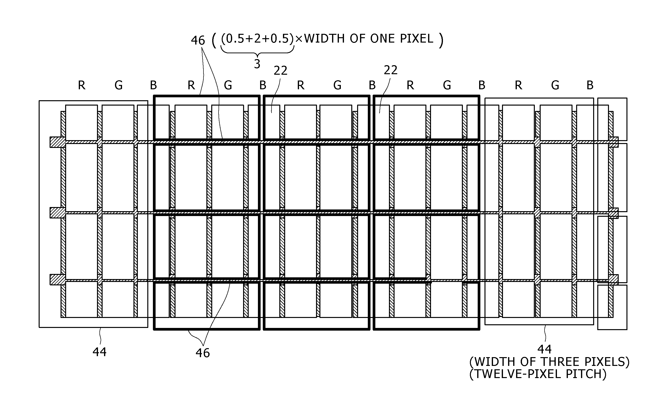
[0113]When there is no layer of a transparent electrode material between detecting electrodes 44 as in the first embodiment, difference in transmittance can occur between colors. In the present embodiment, floating electrodes are arranged to match transmittance between the detecting electrodes 44 to the transmittance of the detecting electrodes 44 themselves.

[0114]FIGS. 9A and 9B and FIGS. 10A and 10B are enlarged plan views showing floating electrodes arranged between detecting electrodes 44.

[0115]As shown in FIGS. 9A and 9B and FIGS. 10A and 10B, floating electrodes 46A are arranged between detecting electrodes 44 to reduce difference in transmittance between colors.

[0116]The floating electrodes 46A in the present embodiment may have a line shape similar to that of detecting electrodes 44, as shown in FIG. 9A. Alternatively, as shown in FIG. 9B, floating electrodes 46 may be arranged in the form of rectangular tiles divided in substantially the size of a pixel....

third embodiment

3. Third Embodiment

[0138]The first and second embodiments bring the transmittance of regions between detecting electrodes close to the transmittance of the detecting electrodes 44 by the arrangement of floating electrodes 46.

[0139]However, a case is assumed in which there is a limitation preventing enlargement of each of the floating electrodes 46 in order to maintain detecting sensitivity, as described above.

[0140]In such a case, it is possible to make the pattern of detecting electrodes 44 resemble the arrangement pattern of floating electrodes 46.

[0141]FIG. 13 and FIGS. 14A and 14B show an example of the pattern of detecting electrodes 44 determined for that purpose. Incidentally, in FIG. 13 and FIGS. 14A and 14B, the detecting electrodes 44 and floating electrodes 46 are not made transparent because making the detecting electrodes 44 transparent renders the figures less easy to view. However, the detecting electrodes 44 and the floating electrodes 46 are formed of a transparent ...


PUM


Abstract

Disclosed herein is a display device including a substrate, a plurality of pixel electrodes arranged in a form of a matrix in a plane parallel with the substrate, a display functional layer exerting an image display function on a basis of an image signal supplied to the plurality of pixel electrodes, a driving electrode opposed to the plurality of pixel electrodes, and a plurality of detecting electrodes arranged in a form of a plane opposed to the driving electrode, separated and arranged at a pitch of a natural number multiple of an arrangement pitch of the pixel electrodes in one direction in the arrangement plane, and each capacitively coupled with the driving electrode.

Description

BACKGROUND OF THE INVENTION[0001]1. Field of the Invention[0002]The present invention relates to a display device having a function of a capacitance type touch sensor (contact detecting device) enabling information input by contact of a finger of a user or the like, and a method of manufacturing the display device.[0003]2. Description of the Related Art[0004]The contact detecting device is generally a device detecting that a finger of a user, a pen or the like comes into contact with or proximity to a detecting surface.[0005]A contact detecting device referred to as a so-called touch panel is known. The touch panel is formed so as to be superimposed on a display panel, and enables information input as a substitute for ordinary buttons by making various buttons displayed as an image on a display surface. Application of this technology to a small mobile device enables a display and a button arrangement to be shared, and provides great advantages of increasing the size of the screen or...

Claims


Application Information

Patent Timeline
IPC IPC(8): G06F3/044H01J9/02G02F1/1343
CPCG02F1/13338G06F3/044G06F3/0412G02F1/134309G06F3/0445G06F3/0446G06F2203/04103G02F1/13306G02F1/133514G02F1/133528
Inventor ISHIZAKI, KOJINOGUCHI, KOUJI
Owner JAPAN DISPLAY INC
Why Eureka
Try Eureka