Non-volatile semiconductor storage device

Active Publication Date: 2010-08-26
KIOXIA CORP
View PDF24 Cites 259 Cited by
  • Summary
  • Abstract
  • Description
  • Claims
  • Application Information

AI Technical Summary

Benefits of technology

[0007]One aspect of the present invention provides a non-volatile semiconductor storage device comprising: a plurality of memory strings each including a plurality of memory transistors connected in series; a plurality of selection transistors each having one end connected to one end of a respective one of the memory strings, each of the selection transistors being conductive when selecting one of the memory strings; and a control circuit performing an erase operation to erase data from a selected one of the memory transistors included in the selected one of the memory strings connected to one end of a selected one of the selection transistors, each of the memory strings comprising: a first semiconductor layer having a columnar portion extending in a vertical direction to a substrate, and functioning as a body of each of the plurality of memory transistors; an electric charge storage layer surrounding the first semiconductor layer; and a first conductive layer surrounding the electric charge storage layer and extending in parallel to the substrate, the first conductive layer functioning as a gate of each of the plurality of memory transistors, each of the selection transistors comprising: a second semiconductor layer in contact with a top surface of the columnar portion and extending in the vertical direction to the substrate, the second semiconductor layer functioning as a body of the selection transistor; a gate insulation layer surrounding the second semiconductor layer; and a second conductive layer surrounding the gate insulation layer and extending in parallel to the substrate, the second conductive layer functioning as a gate of the selection transistor, the control circuit applying a first voltage to the other end of the selected one of the selection transistors, causing the selected one of the selection transistors to turn on, and causing any one of the memory transistors to turn on that is closer to the selection transistor than the selected one of the memory transistors, and also applying a second voltage lower than the first voltage to the gate of the selected one of the memory transistors, and such a potential difference between the first voltage and the second voltage causing a change in electric charges in the electric charge storage layer.
[0008]Another aspect of the present invention provides a non-volatile semiconductor storage device comprising: a plurality of memory strings each including a plurality of memory transistors connected in series; a plurality of first selection transistors each having one end connected to one end of a respective one of the memory strings, each of the first selection transistors being conductive when selecting one of the memory strings; a plurality of second selection transistors each having one end connected to the other end of a respective one of the memory strings, each of the second selection transistors being conductive when selecting one of the memory strings; and a control circuit performing an erase operation to erase...

Problems solved by technology

As such, this erase operation requires w...

Method used


Image

  • Non-volatile semiconductor storage device
  • Non-volatile semiconductor storage device
  • Non-volatile semiconductor storage device

Examples


first embodiment

[0040][Circuit Configuration of Non-Volatile Semiconductor Storage Device in First Embodiment]

[0041]Referring first to FIGS. 1 to 3B, a circuit configuration of a non-volatile semiconductor storage device according to a first embodiment will be described below.

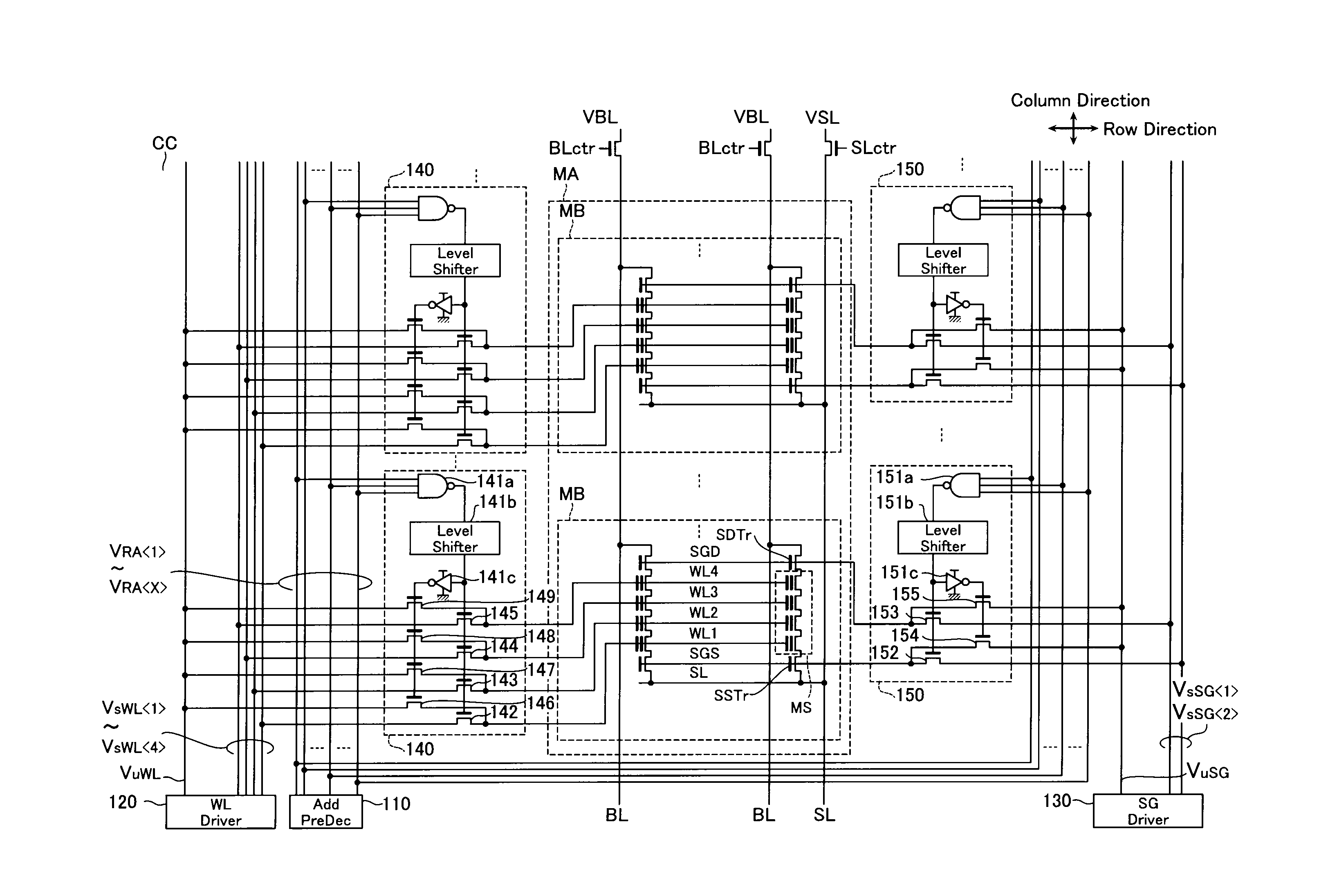
[0042]FIG. 1 is a circuit diagram of the non-volatile semiconductor storage device according to the first embodiment. As illustrated in FIG. 1, the non-volatile semiconductor storage device of the first embodiment comprises a memory cell array MA that stores data, and a control circuit CC that is provided on the periphery thereof and controls the memory cell array MA.

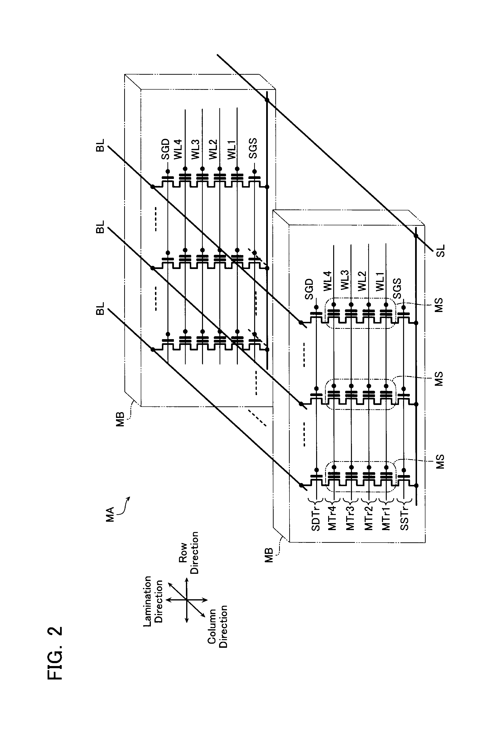
[0043]FIG. 2 is a circuit diagram of one memory cell array MA. As illustrated in FIGS. 1 and 2, the memory cell array MA has a plurality of memory blocks MB aligned in the column direction.

[0044]As illustrated in FIGS. 1 and 2, each memory block MB has memory strings MS, drain-side selection transistors SDTr, and source-side selection transistors SSTr that are ali...

second embodiment

[0124][Circuit Configuration of Non-Volatile Semiconductor Storage Device in Second Embodiment]

[0125]Referring now to FIGS. 9 and 10, a circuit configuration of a non-volatile semiconductor storage device according to a second embodiment will be described below. FIG. 9 is a circuit diagram of the non-volatile semiconductor storage device according to the second embodiment. FIG. 10 is a circuit diagram of one memory cell array MAa according to the second embodiment. Note that the same reference numerals represent the same components as the first embodiment, and description thereof will be omitted in the second embodiment.

[0126]As illustrated in FIG. 9, the non-volatile semiconductor storage device of the second embodiment comprises a memory cell array MAa and a control circuit CCa that are different from the first embodiment.

[0127]As illustrated in FIGS. 9 and 10, each memory cell array MAa has memory blocks MBa different from the first embodiment. Each memory block MBa has memory st...

third embodiment

[0149][Lamination Structure of Non-Volatile Semiconductor Storage Device in Third Embodiment]

[0150]Referring now to FIG. 16, a lamination structure of a non-volatile semiconductor storage device according to a third embodiment will be described below. The third embodiment is different from the first and second embodiments in that it uses a so-called GIDL (Gate Induced Drain Leakage) current for erase operation. FIG. 16 is a partial cross-sectional view of the non-volatile semiconductor storage device of the third embodiment. While the non-volatile semiconductor storage device of the third embodiment has the same circuit configuration as the first embodiment (see FIG. 1), it differs from the first embodiment in how memory cell arrays are laminated and how an erase operation is performed. This is because it utilizes a GIDL current. Note that the same reference numerals represent the same components as the first and second embodiments, and description thereof will be omitted in the thi...


PUM


Abstract

A non-volatile semiconductor storage device includes a control circuit performing an erase operation to erase data from a selected one of memory transistors. The control circuit applies a first voltage to the other end of selected one of selection transistors, causes the selected one of the selection transistors to turn on, and causes any one of the memory transistors to turn on that is closer to the selection transistor than the selected one of the memory transistors. The control circuit also applies a second voltage lower than the first voltage to a gate of the selected one of the memory transistors. Such a potential difference between the first voltage and the second voltage causing a change in electric charges in the electric charge storage layer.

Description

CROSS-REFERENCE TO RELATED APPLICATIONS[0001]This application is based upon and claims the benefit of priority from the prior Japanese Patent Application No. 2009-41157, filed on Feb. 24, 2009, the entire contents of which are incorporated herein by reference.BACKGROUND OF THE INVENTION[0002]1. Field of the Invention[0003]The present invention relates to an electrically rewritable non-volatile semiconductor storage device.[0004]2. Description of the Related Art[0005]As refinement technologies are pushed to the limit for improving the bit density of non-volatile semiconductor storage devices such as NAND type flash memory, there is increasing demand for lamination of memory cells. As one example, there have been proposed lamination-type non-volatile semiconductor storage devices where memory cells are configured with vertical transistors (see, for example, Japanese Patent Laid-Open No. 2007-266143). The lamination-type non-volatile semiconductor storage device comprises a plurality o...

Claims


Application Information

Patent Timeline
IPC IPC(8): G11C16/04G11C11/34
CPCG11C8/08G11C16/0483G11C16/08G11C16/10G11C16/14H01L27/11573H01L27/11578H01L27/11582G11C16/3454H10B43/40H10B43/20H10B43/27H01L27/0688
Inventor HISHIDA, TOMOOIWATA, YOSHIHISAITAGAKI, KIYOTAROMAEDA, TAKASHI
Owner KIOXIA CORP
Why Eureka
Try Eureka