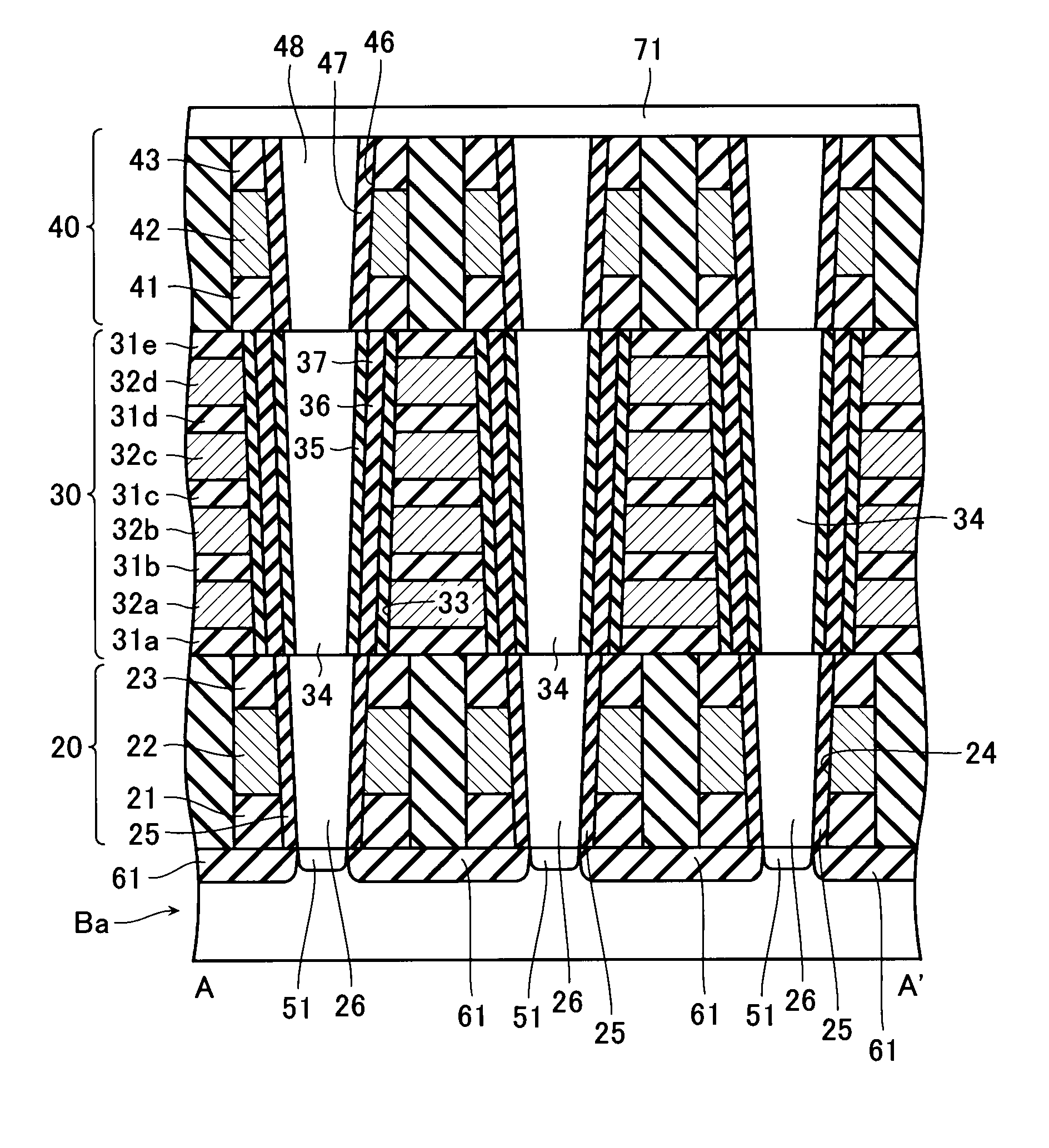
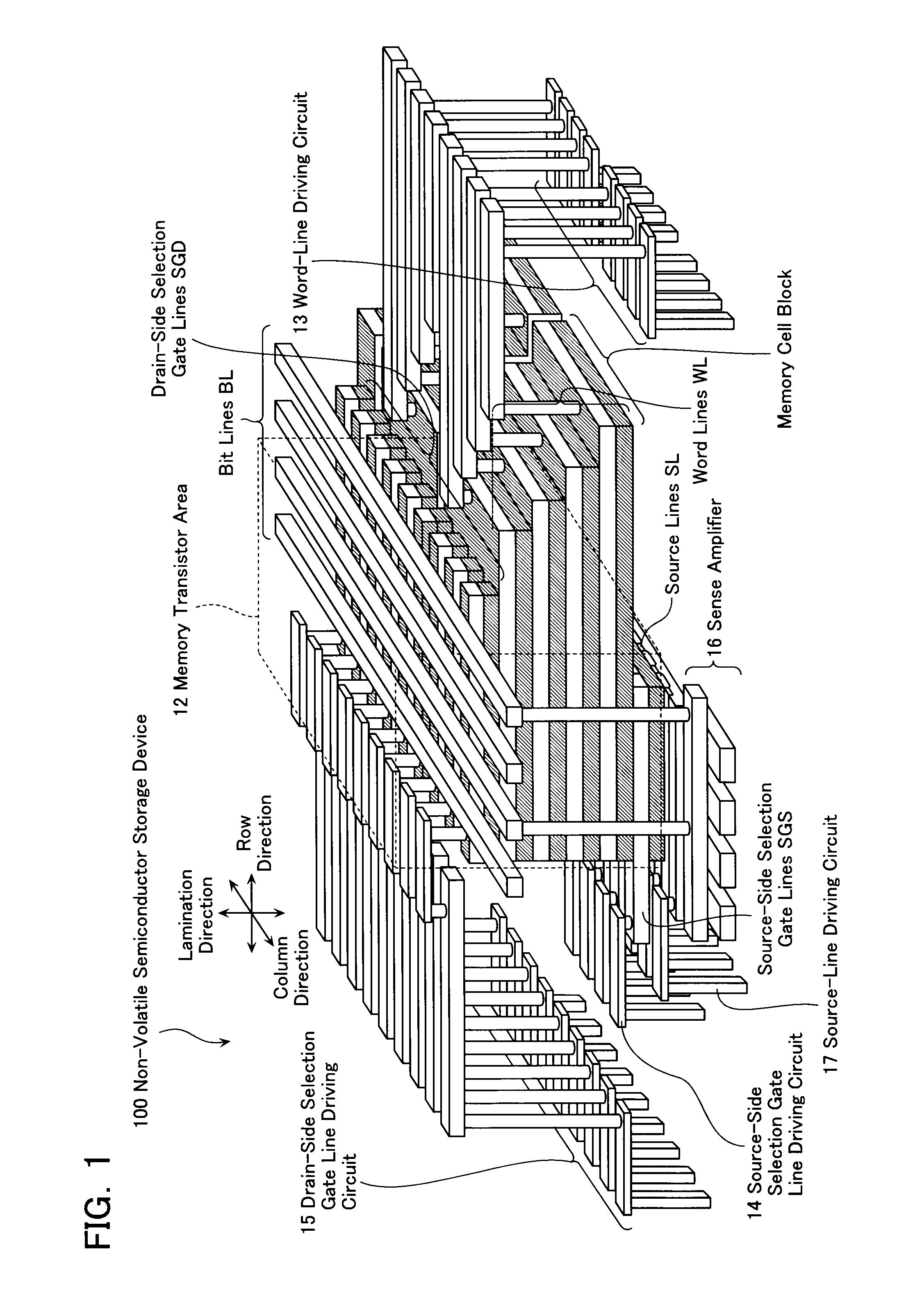
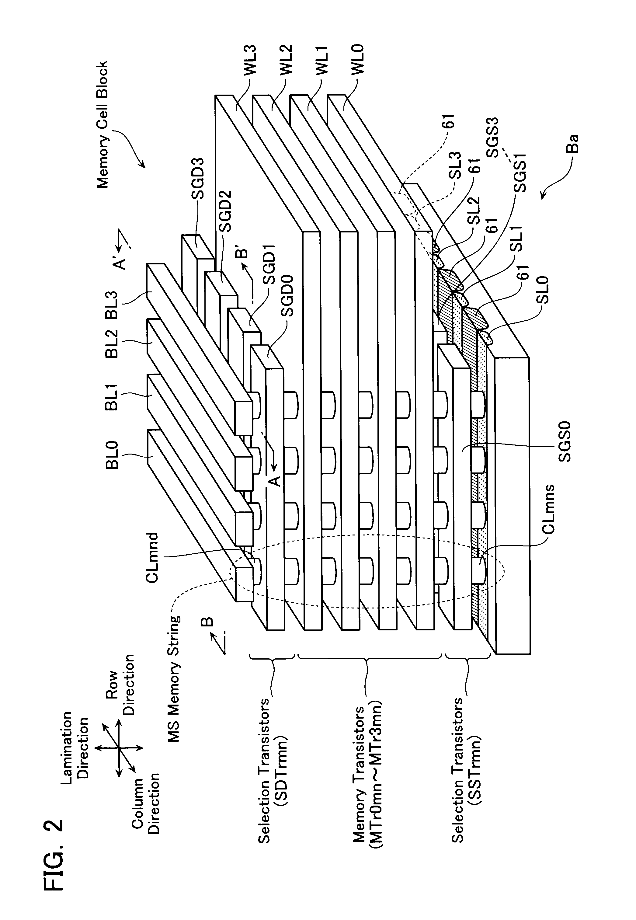
[0007]One aspect of the present invention provides a non-volatile semiconductor storage device comprising: a memory string including a plurality of memory transistors connected in series; a drain-side selection transistor formed at one end of the memory string and operative to be conductive when selecting the memory string; a source-side selection transistor formed at the other end of the memory string and operative to be conductive when selecting the memory string; a bit line connected to the other end of the drain-side selection transistor, the bit line operative to be provided with a voltage corresponding to data to be written to a respective one of the memory transistors and to read a signal read from a respective one of the memory transistors; a source line connected to the other end of the source-side selection transistor; and a control circuit configured to control the memory transistors, the drain-side selection transistor, and the source-side selection transistor to perform read, write, and erase operations on the memory transistors, the memory string comprising: a first semiconductor layer having a columnar portion extending in a vertical direction to a substrate and functioning as a body of a respective one of the plurality of memory transistors; an electric charge accumulation layer formed to surround the first semiconductor layer; and a first conductive layer formed to surround the electric charge accumulation layer and extend in parallel to the substrate, the first conductive layer being laminated to form a plurality of layers and functioning as gates of the plurality of memory transistors, the drain-side selection transistor comprising: a second semiconductor layer in contact with one end of the first semiconductor layer and extending in the vertical direction to the substrate, the second semiconductor layer functioning as a body of the drain-side selection transistor; a second gate insulation layer formed to surround the second semiconductor layer; and a second conductive layer surrounding the second gate insulation layer and extending in parallel to the substrate, the second conductive layer functioning as a gate of the drain-side selection transistor, the source-side selection transistor comprising: a third semiconductor layer in contact with the other end of the first semiconductor layer and extending in the vertical direction to the substrate, the third semiconductor layer functioning as a body of the source-side selection transistor; a third gate insulation layer formed to surround the third semiconductor layer; and a third conductive layer surrounding the third gate insulation layer and extending in parallel to the substrate, the third conductive layer functioning as a gate of the source-side selection transistor, m rows and n columns of the first semiconductor layers arranged on the substrate being included in one memory cell block (where m and n are integers not less than 2), each of the first conductive layers being commonly connected to the (m×n) first semiconductor layers arranged in the one memory cell block, each of the second conductive layers being commonly connected to the n second semiconductor layers arranged along a first direction in the one memory cell block, each of the third conductive layers being commonly connected to the n third semiconductor layers arranged along the first direction in the one memory cell block, each of the bit lines being commonly connected to the m second semiconductor layers arranged along a second direction orthogonal to the first direction in the one memory cell block, each of the source lines being commonly connected to the n third semiconductor layers arranged along the first direction in the one memory cell block, when performing a data erase operation in the one memory cell block, the control circuit being configured to: apply a first voltage to one source line selected from the m source lines in the one memory cell block, while applying a second voltage to the other source lines, the second voltage being equal to a voltage of the source lines before the data erase operation begins; then, after a certain time delay from application of the first voltage, apply a third voltage smaller than the first voltage to the third conductive layer of the source-side selection transistor connected to the selected source line, thereby producing a hole current near the third gate insulation layer due to a potential difference between the first voltage and the third voltage; and apply a fourth voltage to one of the first conductive layers that is connected to the memory transistor to be erased, while bringing the other first conductive layers into a floating state, thereby causing a change in electric charge of the electric charge accumulation layers due to a potential difference between potentials of the first semiconductor layers and the first conductive layers.
[0008]Another aspect of the present invention provides a non-volatile semiconductor storage device comprising: a memory string including a plurality of memory transistors connected in series; a drain-side selection transistor formed at one end of the memory string and operative to be conductive when selecting the memory string; a source-side selection transistor formed at the other end of the memory string and operative to be conductive when selecting the memory string; a bit line connected to the other end of the drain-side selection transistor, the bit line operative to be provided with a voltage corresponding to data to be written to a respective one of the memory transistors and to read a signal read from a respective one of the memory transistors; a source line connected to the other end of the source-side selection transistor; and a control circuit configured to control the memory transistors, the drain-side selection transistor, and the source-side selection transistor to perform read, write, and erase operations on the memory transistors, the memory string comprising: a first semiconductor layer having a columnar portion extending in a vertical direction to a substrate and functioning as a body of a respective one of the plurality of memory transistors; an electric charge accumulation layer formed to surround the first semiconductor layer; and a first conductive layer formed to surround the electric charge accumulation layer and extend in parallel to the substrate, the first conductive layer being laminated to form a plurality of layers and functioning as gates of the plurality of memory transistors, the drain-side selection transistor comprising: a second semiconductor layer in contact with one end of the first semiconductor layer and extending in the vertical direction to the substrate, the second semiconductor layer functioning as a body of the drain-side selection transistor; a second gate insulation layer formed to surround the second semiconductor layer; and a second conductive layer surrounding the second gate insulation layer and extending in parallel to the substrate, the second conductive layer functioning as a gate of the drain-side selection transistor, the source-side selection transistor comprising: a third semiconductor layer in contact with the other end of the first semiconductor layer and extending in the vertical direction to the substrate, the third semiconductor layer functioning as a body of the source-side selection transistor; a third gate insulation layer formed to surround the third semiconductor layer; and a third conductive layer surrounding the third gate insulation layer and extending in parallel to the substrate, the third conductive layer functioning as a gate of the source-side selection transistor, m rows and n columns of the (m×n) first semiconductor layers arranged on the substrate being included in one memory cell group (where m and n are integers not less than 2), each of the first conductive layers being commonly connected to the n first semiconductor layers aligned along a first direction in the one memory cell group, each of the second conductive layers being commonly connected to the n second semiconductor layers arranged along the first direction in the one memory cell group, each of the third conductive layers being commonly connected to the n third semiconductor layers arranged along the first direction in the one memory cell group, each of the bit lines being commonly connected to the m second semiconductor layers arranged along a second direction orthogonal to the first direction in the one memory cell group, each of the source lines being commonly connected to the (m×n) third semiconductor layers in the one memory cell group, when performing a data erase operation in the one memory cell group, the control circuit being configured to: apply a first voltage to one of the source lines that is disposed in the memory cell group in which the memory transistor to be erased is present; then, after a certain time delay from application of the first voltage, apply a second voltage smaller than the first voltage to one of the m third conductive layers in the one memory cell group that is connected to the source-side selection transistor corresponding to the memory transistor to be erased, thereby producing a hole current near the third gate insulation layer due to a potential difference between the first voltage and the second voltage, while applying a third voltage to the other third conductive layers, the third voltage being equal to a voltage of the third conductive layers before the data erase operation begins; and apply a fourth voltage to one of the first conductive layers that is connected to the memory transistor to be erased, while bringing the other first conductive layers into a floating state, thereby causing a change in electric charge of the electric charge accumulation layers due to a potential difference between potentials of the first semiconductor layers and the first conductive layers.

