Semiconductor device and method of manufacturing the same

a semiconductor and semiconductor technology, applied in semiconductor devices, diodes, electrical devices, etc., can solve the problems of limiting the improvement of cutoff performance by thinning the channel, the mobility of the channel cannot be increased, and the difficulty of completely depleting the surface channel region, etc., to achieve the effect of lifting the mobility and not increasing the mobility of the channel

Inactive Publication Date: 2005-01-20
NISSAN MOTOR CO LTD
View PDF3 Cites 116 Cited by
  • Summary
  • Abstract
  • Description
  • Claims
  • Application Information

AI Technical Summary

Problems solved by technology

This raises a problem that channel mobility cannot be increased.
Accordingly, if the impurity concentration of the surface channel region is increased, it will be difficult to completely deplete the surface channel region.
Hei-6-252408, the accuracy of processing limits a channel thickness, and therefore, there is a limit on improving cutoff performance by thinning the channel.

Method used


Image

  • Semiconductor device and method of manufacturing the same
  • Semiconductor device and method of manufacturing the same
  • Semiconductor device and method of manufacturing the same

Examples


second embodiment

(Second Embodiment)

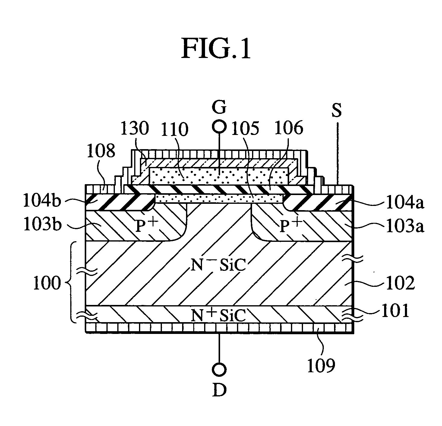
FIG. 5 is a sectional view showing a semiconductor device according to a second embodiment of the present invention. The semiconductor device has an n+-type substrate region 101 and an n−-type drain region 102 formed on the substrate region 101. The drain region 102 has a lower impurity concentration than the substrate region 101. At the surface of the drain region 102, p−-type base regions 103a and 103b are formed. At predetermined locations on the surfaces of the base regions 103a and 103b, trenches 132a, 132b, and 132c are formed through the base regions 103a and 103b up to the drain region 102. At predetermined locations on the surfaces of the base regions 103a and 103b, n+-type source regions 104a and 104b are formed. On the inner side walls of the trenches 132a, 132b, and 132c and on the base regions 103a and 103b, n−-type surface channel regions 105a, 105b, and 105c are formed to connect the source regions 104a and 104b to the drain region 102. On the surfa...

third embodiment

(Third Embodiment)

FIG. 6 is a sectional view showing a semiconductor device according to a third embodiment of the present invention. The semiconductor device has an n+-type substrate region 101 and a p−type epitaxial layer 120 formed on the substrate region 101. The epitaxial layer 120 has a lower impurity concentration than the substrate region 101. At predetermined locations on the surface of the epitaxial layer 120, an n+-type source region 104 and an n+-type drain region 112 are formed. On the surface of the epitaxial layer 120, there is formed an n−-type surface channel region 105 to connect the source region 104 to the drain region 112. On the surface channel region 105, a gate insulating film 106 is formed, and on the gate insulating film 106, a gate electrode 110 is formed from a p+-type polysilicon carbide which is a semiconductor material having a work function of 5.1 eV or over. In contact with the source region 104, a source electrode 108 is formed. In contact with the ...

fourth embodiment

(Fourth Embodiment)

FIGS. 7 and 8 show a semiconductor device according to a fourth embodiment of the present invention. This semiconductor device employs a silicon substrate.

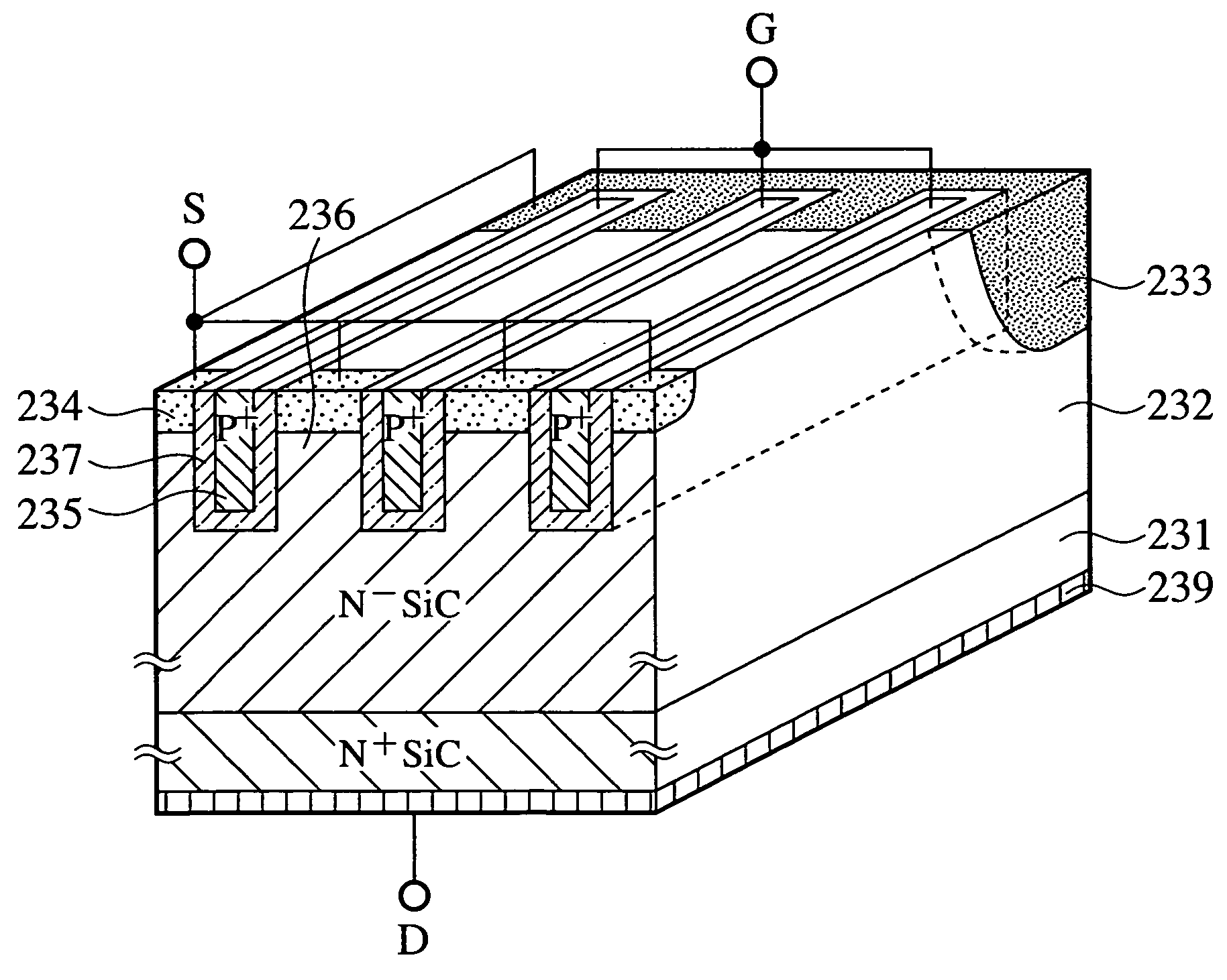
FIG. 7 is a perspective view showing the semiconductor device of the fourth embodiment and FIG. 8 is a sectional view showing the same. For the sake of clear explanation, FIG. 7 strips off a metal film serving as a surface electrode and a surface protection film. It is naturally possible to employ these metal film electrode and surface protection film. The semiconductor device has an n+-type substrate region 201, an n-type drain region 202, an n+-type source region 204, an insulating film 207, an insulated electrode 205, and a p-type base region 203. The insulating film 207 and insulated electrode 205 are formed in a U-shape in a trench having substantially vertical side walls. The insulated electrode 205 is insulated from the drain region 202 by the insulating film 207. In FIG. 7, the source region 204 is in c...


PUM


Abstract

An aspect of the present invention provides a semiconductor device that includes a semiconductor base including, a semiconductor substrate of a first conductivity type and a drain region of the first conductivity type formed on the semiconductor substrate and having a lower impurity concentration than the semiconductor substrate, a gate electrode insulated from the semiconductor base by a gate insulating film, the gate electrode made of a semiconductor material, a built-in potential difference between a region and the gate electrode made of the semiconductor material is greater than that of polysilicon having as high impurity concentration as possible, the region is a part of the drain region adjacent to the gate electrode through the gate insulating film.

Description

BACKGROUND OF THE INVENTION The present invention relates to a semiconductor device and a method of manufacturing the same. An example of a planar power MOSFET semiconductor device is disclosed in Japanese Laid-Open Patent Publication No. Hei-10-308510. In this publication, the semiconductor device has an n+-type silicon carbide semiconductor substrate, an n− type silicon carbide epitaxial layer formed on the substrate and having a lower impurity concentration than the substrate, a p− type base region formed in a predetermined area at the surface of the epitaxial layer, and an n+-type source region formed in a predetermined area at the surface of the base region. At the surface of the base region, an n-type surface channel region is formed to connect the source region and epitaxial layer to each other. On the surface channel region, there is formed a gate insulating film on which a gate electrode is formed from p+-type polysilicon. In contact with the source region, a source electr...

Claims


Application Information

Patent Timeline
Patent Type & Authority Applications(United States)
IPC IPC(8): H01L21/04H01L29/24H01L29/267H01L29/49H01L29/739H01L29/78
CPCH01L29/1608H01L29/4966H01L29/66068H01L29/739H01L29/78H01L29/165H01L29/7804H01L29/7813H01L29/7838H01L29/7828H01L29/7802
Inventor TANAKA, HIDEAKIHOSHI, MASAKATSUHAYASHI, TETSUYAKANEKO, SAICHIROU
Owner NISSAN MOTOR CO LTD
Why Eureka
Try Eureka