Fabrication of Source/Drain Extensions with Ultra-Shallow Junctions

a technology of source/drain extension and ultra-shallow junction, which is applied in the manufacturing of semiconductor/solid-state devices, basic electric elements, electric devices, etc., can solve the problems of increasing leakage current, preventing further improvement of device performance, and causing problems such as affecting the performance of the device, so as to reduce the junction depth and reduce the resistance of the sheet. , the effect of reducing the leakage curren

Active Publication Date: 2010-08-26
TAIWAN SEMICON MFG CO LTD
View PDF12 Cites 12 Cited by
  • Summary
  • Abstract
  • Description
  • Claims
  • Application Information

AI Technical Summary

Benefits of technology

[0008]The advantageous features of the present invention include reduced sheet resistance and reduced junction depth in source and drain extension regions, and reduced leakage currents compared to the commonly used Ge PAI method.

Problems solved by technology

Second, in the amorphized substrate, atoms are arranged randomly, and hence the subsequently implanted p-type or n-type impurities cannot channel through the spaces between the periodically located atoms to reach a great depth.
The PAI, however, also incurs problems.
For example, after the activation, residue defects may still exist and will cause an increase in leakage currents.
Such leakage currents prevent further improvement of device performance.

Method used


Image

  • Fabrication of Source/Drain Extensions with Ultra-Shallow Junctions
  • Fabrication of Source/Drain Extensions with Ultra-Shallow Junctions
  • Fabrication of Source/Drain Extensions with Ultra-Shallow Junctions

Examples


Embodiment Construction

[0016]The making and using of the embodiments of the present invention are discussed in detail below. It should be appreciated, however, that the embodiments provide many applicable inventive concepts that can be embodied in a wide variety of specific contexts. The specific embodiments discussed are merely illustrative of specific ways to make and use the invention, and do not limit the scope of the invention.

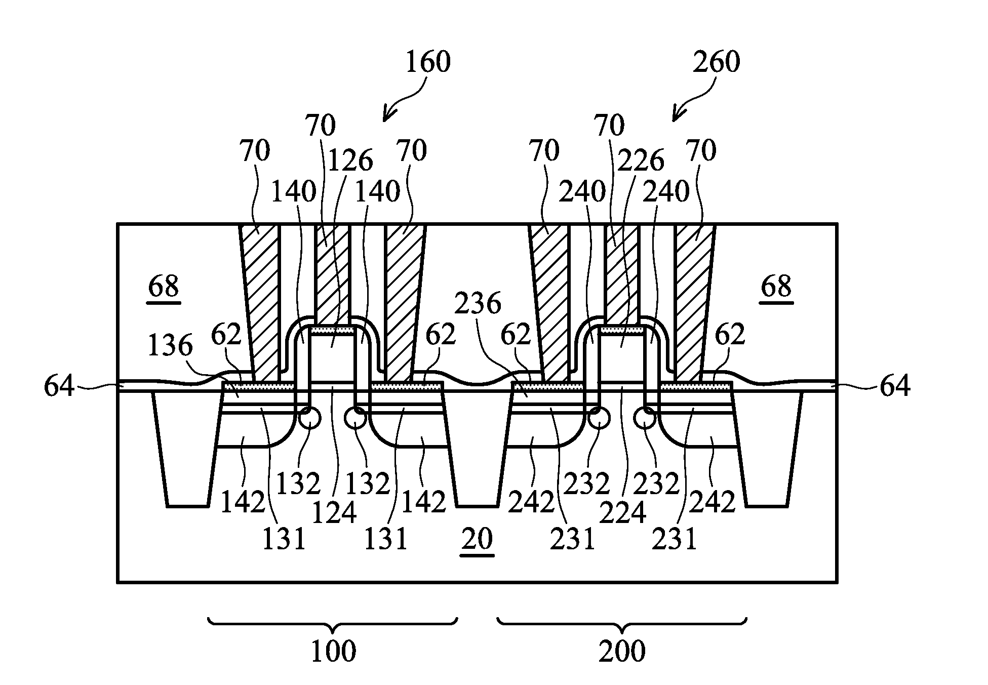
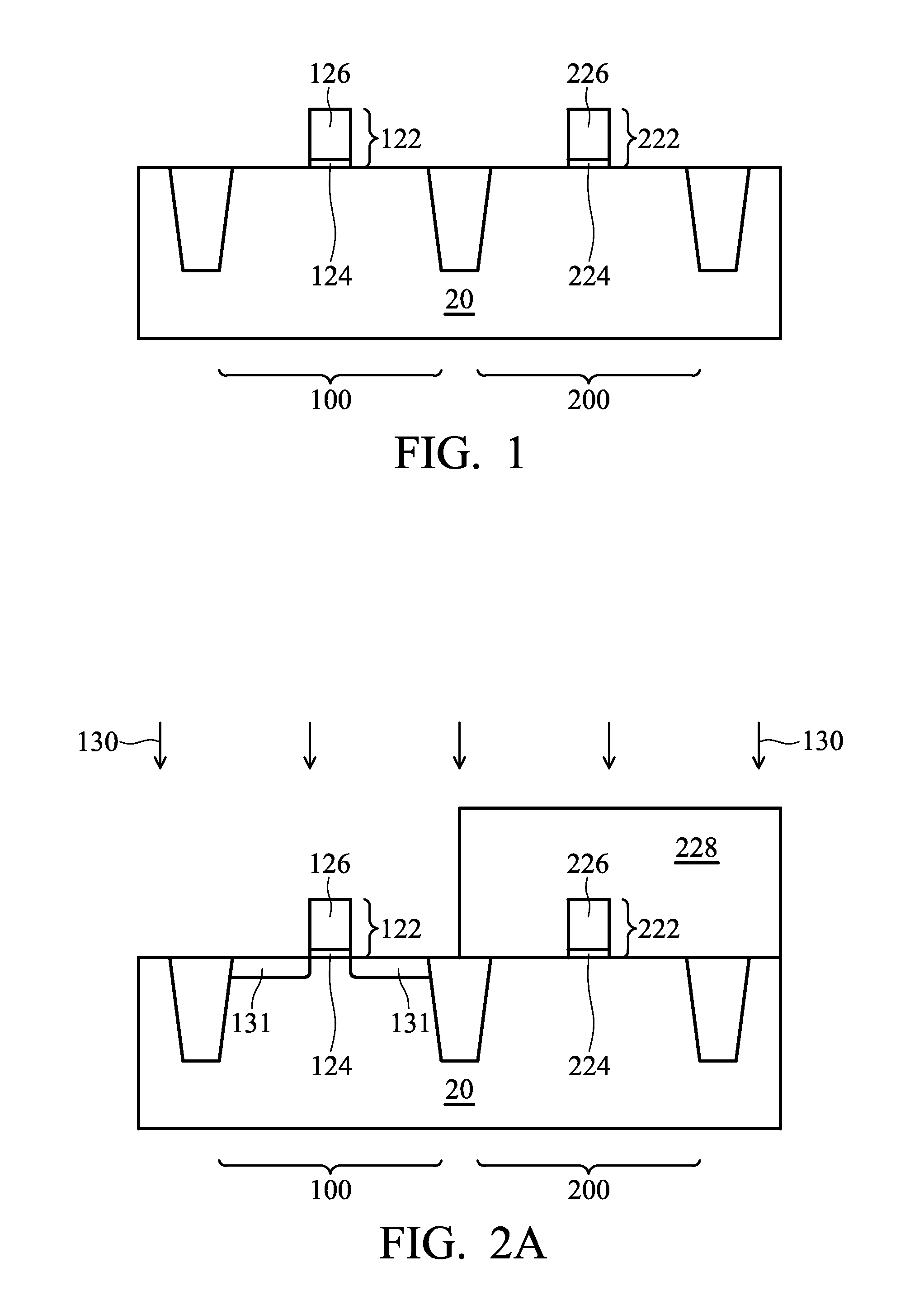
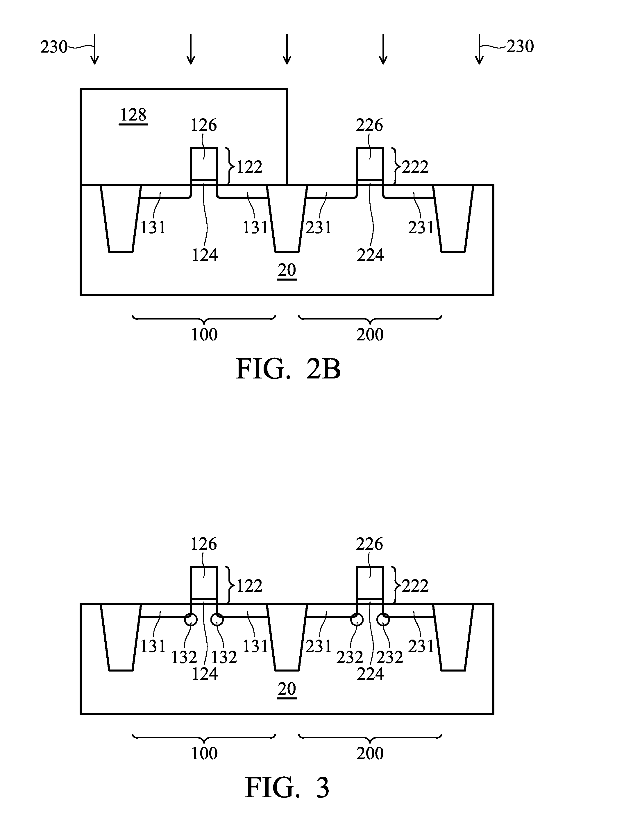
[0017]Conventionally, pre-amorphized implantation (PAI) was performed by implanting germanium ions into silicon substrates. However, it has been found that the metal-oxide-semiconductor (MOS) device formed using germanium PAI can no longer provide low sheet resistances, small junction depths, and low leakage currents that satisfy the demanding requirements of 32 nm and 22 nm technologies. A novel method for forming MOS devices and performing the PAI is thus provided. The intermediate stages of manufacturing an embodiment of the present invention are illustrated. The variations ...


PUM


Abstract

A method of forming an integrated circuit device includes providing a semiconductor substrate; forming a gate structure on the semiconductor substrate; and performing a pre-amorphized implantation (PAI) by implanting a first element selected from a group consisting essentially of indium and antimony to a top portion of the semiconductor substrate adjacent to the gate structure. The method further includes, after the step of performing the PAI, implanting a second element different from the first element into the top portion of the semiconductor substrate. The second element includes a p-type element when the first element includes indium, and includes an n-type element when the first element includes antimony.

Description

[0001]This application claims the benefit of U.S. Provisional Application No. 61 / 154,667 filed on Feb. 23, 2009, entitled “Fabrication of Source / Drain Extensions with Ultra-Shallow Junctions,” which application is hereby incorporated herein by reference.TECHNICAL FIELD[0002]This invention relates generally to semiconductor devices, and more particularly to metal-oxide-semiconductor (MOS) devices, and even more particularly to MOS devices having ultra-shallow junctions and methods for forming the same.BACKGROUND[0003]With the increasing down-scaling of integrated circuits, there exist increasingly demanding requirements for reducing the sheet resistance of source and drain regions of metal-oxide-semiconductor (MOS) devices, and particularly the sheet resistance of source and drain extension regions. Reduced sheet resistances in the source and drain extension regions may help increase carrier mobility, hence resulting in increased drive currents.[0004]To reduce the sheet resistance of...

Claims


Application Information

Patent Timeline
Patent Type & Authority Applications(United States)
IPC IPC(8): H01L21/8238H01L21/336
CPCH01L21/823814
Inventor CHIU, YIHANGFU, CHU-YUN
Owner TAIWAN SEMICON MFG CO LTD
Why Eureka
Try Eureka