Plasma processing apparatus
- Summary
- Abstract
- Description
- Claims
- Application Information
AI Technical Summary
Benefits of technology
Problems solved by technology
Method used
Image

Examples
first exemplary embodiment
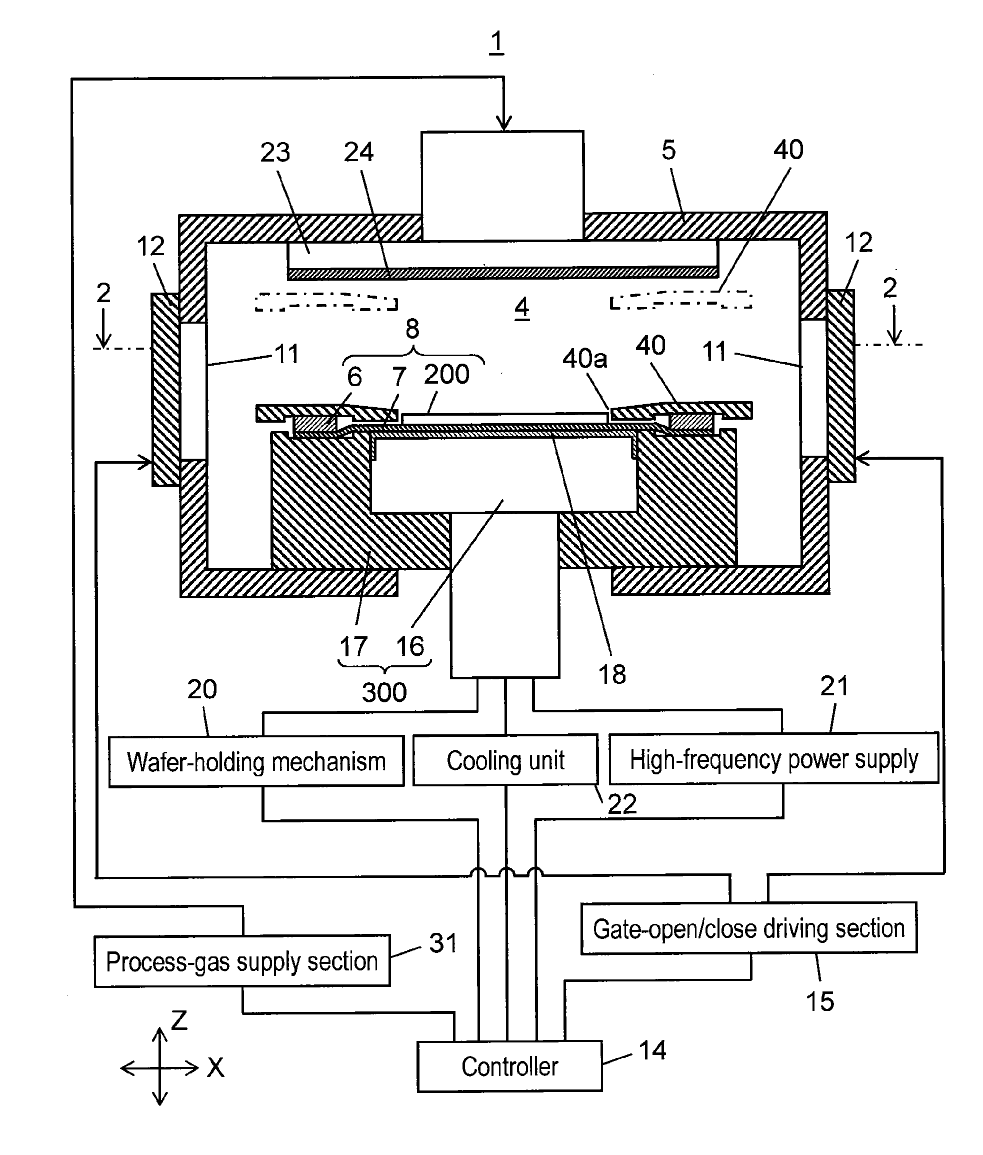
[0036]An exemplary embodiment of the present invention is described hereinafter with reference to the accompanying drawings.
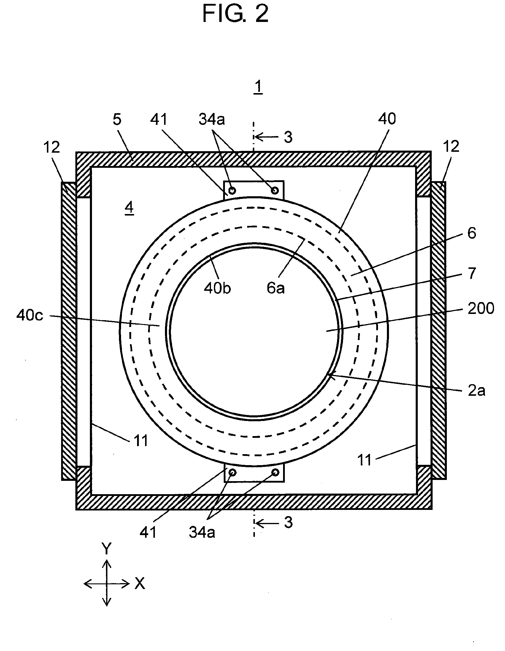
[0037]FIG. 1 is a sectional front view of the plasma processing device in accordance with the exemplary embodiment of the present invention. FIG. 2 is a sectional plan view of the plasma processing device in accordance with the exemplary embodiment. FIG. 3 is a sectional side view of the plasma processing device in accordance with the exemplary embodiment.
[0038]As is shown in FIGS. 1, 2 and 3, plasma processing device 1 has stage 300, on which semiconductor wafer (hereinafter referred to simply as a wafer) 200 as an object to be treated is mounted, and vacuum chamber 5 that covers stage 300 and forms enclosed space 4 therein. FIG. 2 is a sectional view taken along the line 2-2 of FIG. 1. FIG. 3 is a sectional view taken along the line 3-3 of FIG. 2.
[0039]Wafer 200 is attached on the upper surface of adhesive sheet 7 whose periphery is held by holder frame 6 mad...
PUM
| Property | Measurement | Unit |
|---|---|---|
| Dielectric polarization enthalpy | aaaaa | aaaaa |
| Area | aaaaa | aaaaa |
| Distance | aaaaa | aaaaa |
Abstract
Description
Claims
Application Information
 - Generate Ideas
- Intellectual Property
- Life Sciences
- Materials
- Tech Scout
- Unparalleled Data Quality
- Higher Quality Content
- 60% Fewer Hallucinations
Browse by: Latest US Patents, China's latest patents, Technical Efficacy Thesaurus, Application Domain, Technology Topic, Popular Technical Reports.
© 2025 PatSnap. All rights reserved.Legal|Privacy policy|Modern Slavery Act Transparency Statement|Sitemap|About US| Contact US: help@patsnap.com