
Imaging apparatus and method

a technology of imaging apparatus and slit, which is applied in the field of imaging apparatus and methods, can solve the problems of little practical use of pinhole cameras, and achieve the effects of reducing the size, weight and reducing the cost of imaging apparatus, and being dynami

Inactive Publication Date: 2010-09-02
SONY SEMICON SOLUTIONS CORP
View PDF20 Cites 4 Cited by
  • Summary
  • Abstract
  • Description
  • Claims
  • Application Information

AI Technical Summary

Benefits of technology

This solution enables a compact, lightweight, and cost-effective imaging device capable of capturing clear images with the desired amount of light, effectively utilizing the dynamic range of the imaging device, especially in low light conditions and wide dynamic range scenarios.

Problems solved by technology

In imaging under low light conditions, particularly, in dark places, the pinhole camera is of little practical use.

Method used


Image

  • Imaging apparatus and method
  • Imaging apparatus and method
  • Imaging apparatus and method

Examples


first example

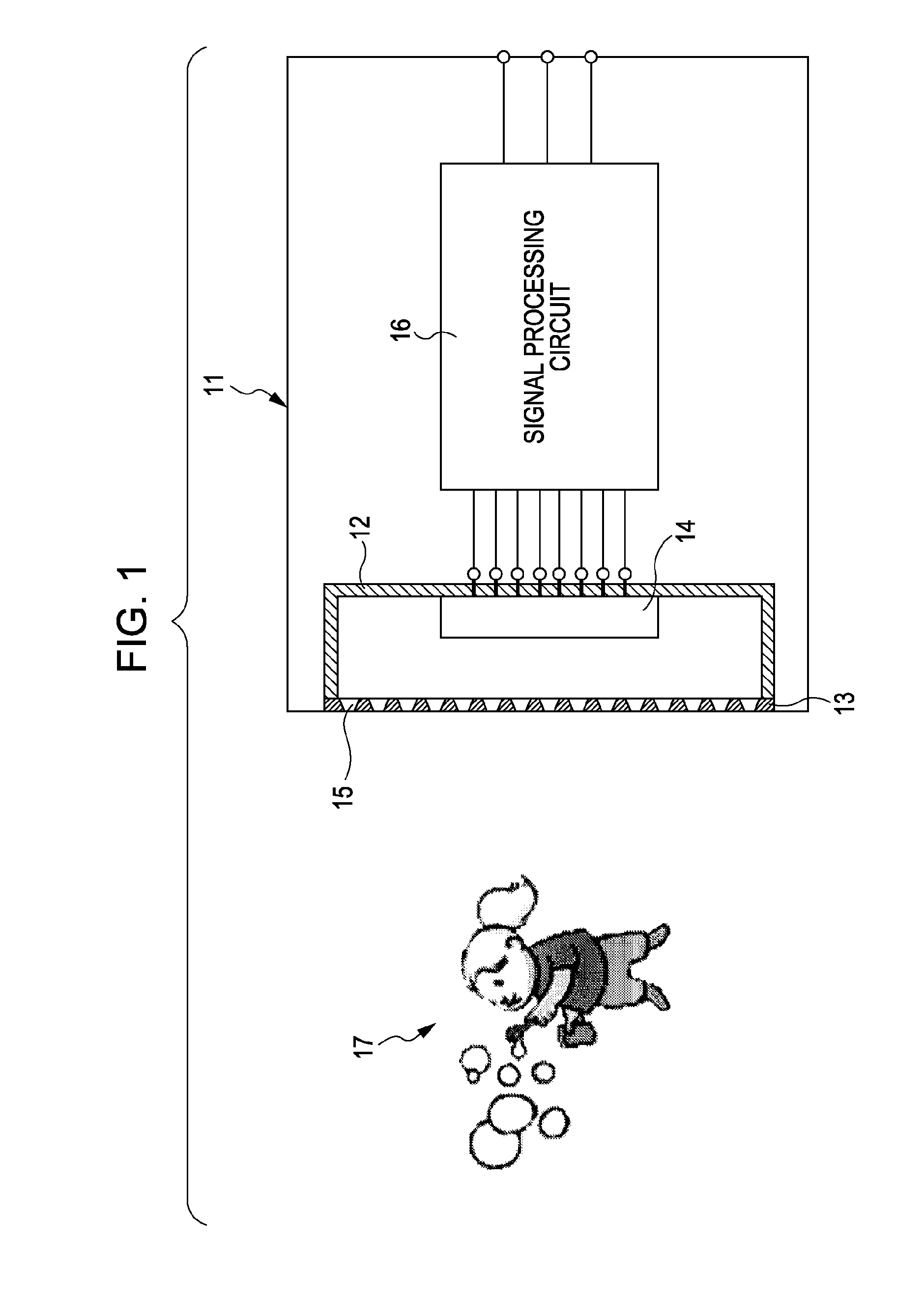
[0052]FIG. 4 is a cross-sectional view illustrating the cross-sectional shape of each aperture 15A according to a first example. In the first example, the cross-sectional area of each aperture 15A is uniform in the direction from the subject 17 to the imaging device 14, i.e., in the direction from the surface of the light shielding plate 13 close to the subject 17 to the surface thereof close to the imaging device 14. In addition, the axis O of each aperture 15A is orthogonal to the surface of the light shielding plate 13. In other words, the apertures 15 have the same shape.

second example

[0053]FIG. 5 is a cross-sectional view illustrating the cross-sectional shape of each aperture 15B according to a second example. In the second example, the cross-sectional area of each aperture 15B is uniform in the direction from the surface of the light shielding plate 13 close to the subject 17 to the surface thereof close to the imaging device 14 such that the axes O of the respective apertures 15B are converged to the imaging device 14. In other words, the inclination of the axis O of each aperture 15B depends on the position of the aperture 15B. Therefore, the shape of the aperture 15B depends on the position thereof.

third example

[0054]FIG. 6 is a cross-sectional view illustrating the cross-sectional shape of each aperture 15C according to a third example. In the third example, the cross-sectional area of each aperture 15C is uniform in the direction from the surface of the light shielding plate 13 close to the subject 17 to the surface thereof close to the imaging device 14 such that the axes O of the respective apertures 15C are diverged toward the imaging device 14. In other words, the inclination of the axis O of each aperture 15C depends on the position of the aperture 15C. Therefore, the shape of the aperture 15C depends on the position thereof.


PUM


Abstract

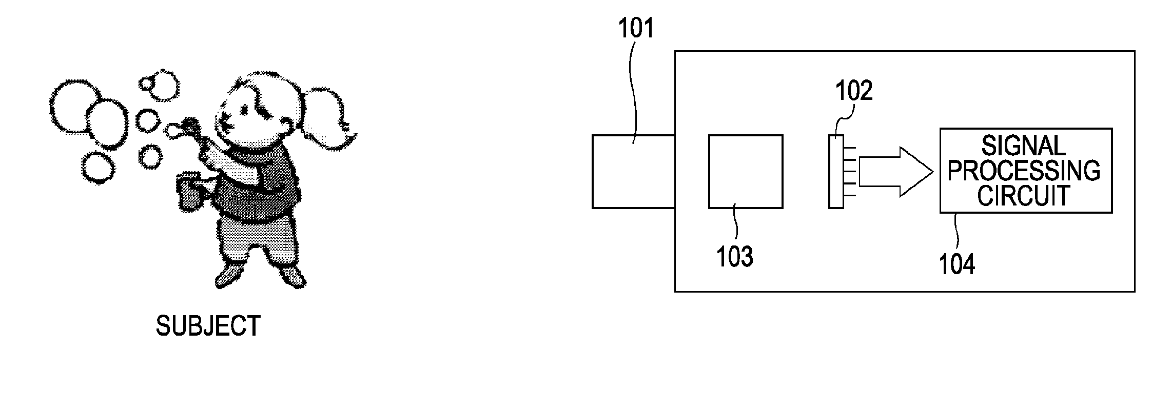
An imaging apparatus includes an imaging device, a light guide mechanism, and a signal processing unit. The imaging device converts light incident on a photoelectric conversion portion of the imaging device into electric signals. The light guide mechanism, arranged adjacent to the photoelectric conversion portion of the imaging device, includes a plurality of apertures that guide light from a subject to the photoelectric conversion portion of the imaging device. The signal processing unit performs desired signal processing on the electric signals output from the imaging device on the basis of subject information units derived from the light guided onto the photoelectric conversion portion of the imaging device through the apertures.

Description

[0001]This application is a continuation of U.S. patent application Ser. No. 11 / 626,950, filed Jan. 25, 2007, which is a continuation-in-part of U.S. patent application Ser. No. 11 / 208,377, filed Aug. 19, 2005, the entireties of which are incorporated herein by reference to the extent permitted by law. The present application claims priority to Japanese patent application No. JP 2004-240605 filed in the Japanese Patent Office on Aug. 20, 2004 and Japanese Patent Application No. JP 2005-237139 filed in the Japanese Patent Office on Aug. 18, 2005, the entire contents both of which are incorporated by reference herein to the extent permitted by law.BACKGROUND OF THE INVENTION[0002]The present invention relates to imaging apparatuses and methods, and in particular, to an imaging apparatus using an imaging device that converts light from a subject into electric signals and a method of imaging thereof.[0003]As an imaging apparatus, a pinhole camera is well-known. In the pinhole camera, li...

Claims


Application Information

Patent Timeline
Patent Type & Authority Applications(United States)
IPC IPC(8): H04N9/68H04N23/12G02B5/00G03B15/00H04N23/40H04N23/76
CPCH04N5/2254H04N3/1593G03B9/04H04N25/41
Inventor NARABU, TADAKUNI
Owner SONY SEMICON SOLUTIONS CORP
Learn More