Biochip

Inactive Publication Date: 2010-09-02
SUMITOMO BAKELITE CO LTD +1
View PDF3 Cites 7 Cited by
  • Summary
  • Abstract
  • Description
  • Claims
  • Application Information

AI Technical Summary

Benefits of technology

[0009]According to the present invention, since a height position of a height measurement point set on the upper surface of a substrate is measured such that a measurement result is output as substrate height data, and, at the time of performing a placing step, a control parameter for controlling a component

Problems solved by technology

However, in a conventional device disclosed in JP-A-2002-134899, the mounting position precision in the horizontal direction is detected and corrected, but position precision in a height direction is not detected and corrected.
To this end, when the substrate has a thickness variation or curvature deformation, the elec

Method used


Image

  • Biochip
  • Biochip
  • Biochip

Examples


Example

[0020]Next, embodiments of the present invention will be described with reference to the accompanying drawings.

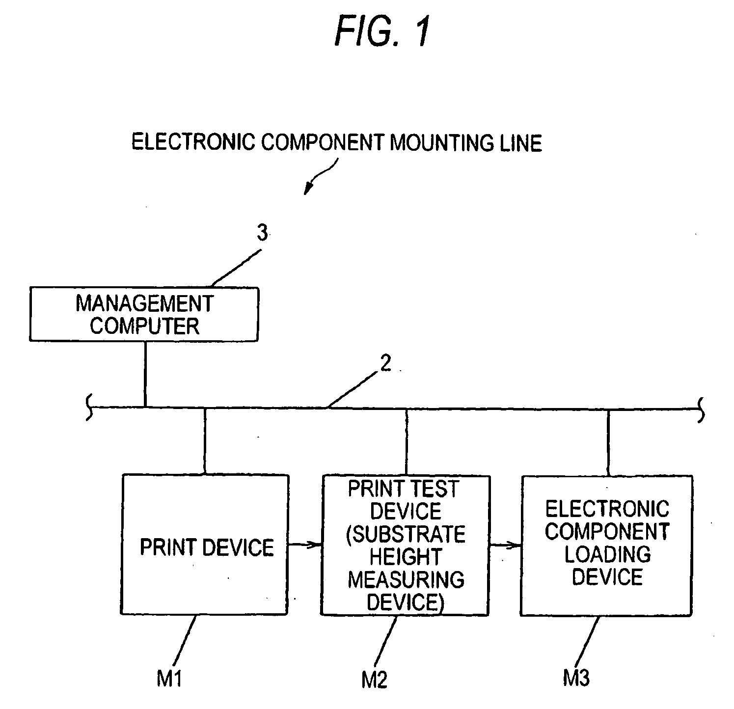
[0021]First, the electronic component mounting system will be described with reference to FIG. 1. In FIG. 1, in the electronic component mounting system, an electronic component mounting line 1 includes a print device M1, a print test device M2, and an electronic component placing device M3, all of which are electronic component mounting devices and connected to one another by a communication network 2, and controlled by a management computer 3. By the plurality of electronic component mounting devices, an electronic component is mounted on a substrate to manufacture a mounting substrate.

[0022]The print device M1 screen-prints a soldering paste for joining the electronic component on an electrode of the substrate. The print test device M2 tests a print state of the printed soldering paste, detects a height position of a height measurement point set on the upper surface of t...


PUM

PropertyMeasurementUnit
Speedaaaaaaaaaa
Heightaaaaaaaaaa

Abstract

To provide an electronic component mounting system and an electronic component mounting method which can prevent a mounting failure due to positional error in a height direction of a substrate and ensure mounting quality. The electronic component mounting system includes a plurality of electronic component mounting devices connected to one another and mounts an electronic component on a substrate to manufacture a mounting substrate. A print test device for testing the substrate after solder printing measures a height position of a height measurement point set on the upper surface of the substrate 4 by a height measuring machine 22 and outputs a measurement result as substrate height data. In a component placing step using an electronic component placing device, a control parameter for controlling a component placing operation of the placing head 32 is updated. Accordingly, it is possible to correct a variation of the height position of an individual substrate and to prevent a mounting failure due to positional error in the height direction of the substrate.

Description

TECHNICAL FIELD[0001]The present invention relates to an electronic component mounting system and an electronic component mounting method for mounting an electronic component on a substrate.BACKGROUND ART[0002]An electronic component mounting system for mounting an electronic component on a substrate by solder joint to manufacture a mounting substrate includes a plurality of electronic component mounting devices such as a solder print device, an electronic component placing device, and a reflow device, all of which are connected to one another. Such an electronic component mounting system, an electronic component mounting line having a test function, such as a configuration of arranging test devices between devices, is introduced in order to reliably manage quality (for example, see Japanese Patent Publication JP-A-2002-134899).[0003]In the example disclosed in JP-A-2002-134899, a print test device is arranged between a print device and an electronic component placing device, and, w...

Claims


Application Information

Patent Timeline
IPC IPC(8): C40B30/04C40B99/00C40B60/12C40B40/08C40B40/10C40B40/12C40B50/18C12Q1/00G01N33/53G01N37/00
CPCC12Q1/003G01N33/53G01N37/00C12Q1/6837
Inventor ISHIHARA, KAZUHIKOFUNAOKA, SOHEIYOKOYAMA, KANEHISA
Owner SUMITOMO BAKELITE CO LTD
Why Eureka
Try Eureka