Wafer processing tape
a technology of wafers and processing tapes, applied in the direction of film/foil adhesives, chemistry apparatuses and processes, etc., can solve the problems of troublesome actual use of tapes, difficult to suppress transfer marks, and problems in semiconductor wafer processing, etc., to reduce voids, reduce voids, and reduce the effect of size changes
- Summary
- Abstract
- Description
- Claims
- Application Information
AI Technical Summary
Benefits of technology
Problems solved by technology
Method used
Image

Examples
first embodiment
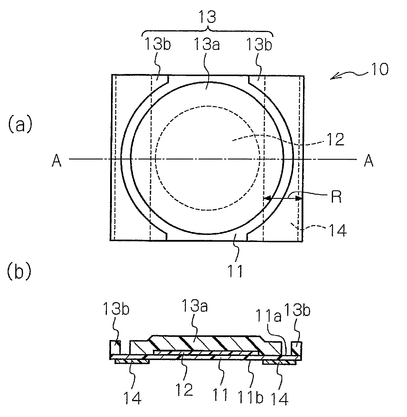
[0047]An explanation of a wafer processing tape according to a first embodiment of the present invention will be explained in detail with reference to the attached drawings.
[0048]FIG. 1(a) is a plan view showing a wafer processing tape according to a first embodiment of the present invention, and FIG. 1(b) is a sectional view taken along the line A-A of FIG. 1(a).
[0049]As shown in FIGS. 1(a) and 1(b), a wafer processing tape 10 includes a release film 11 having a relatively long length, an adhesive layer 12, a pressure-sensitive adhesive film 13, and a support member 14.
[0050]The adhesive layer 12 is formed on a first surface 11a of the release film 11 and has a round label shape corresponding to the shape of the semiconductor wafer. The pressure-sensitive adhesive film 13 has a round label portion 13a adopted to cover the adhesive layer 12 in such a manner as to be brought into contact with the release film 11 around the adhesive layer 12 and a surrounding portion 13b adopted to su...
second embodiment
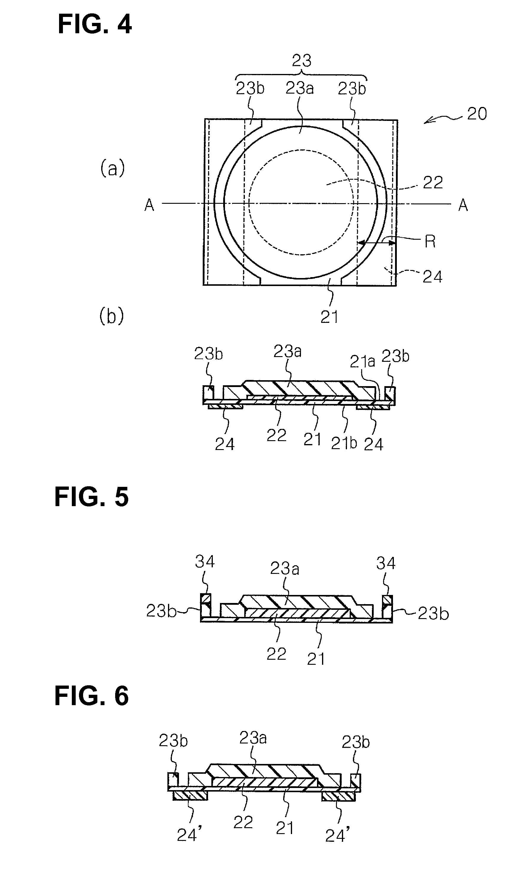
[0089]An explanation of a wafer processing tape according to a second embodiment of the present invention will be explained in detail with reference to the attached drawings.
[0090]FIG. 4(a) is a plan view showing a wafer processing tape according to a second embodiment of the present invention, and FIG. 4(b) is a sectional view taken along the line A-A of FIG. 4(a).
[0091]As shown in FIGS. 4(a) and 4(b), a wafer processing tape 20 according to the present invention includes a release film 21 having a relatively long length, an adhesive layer 22, a pressure-sensitive adhesive film 23, and a colored support member 24.
[0092]The adhesive layer 22 is formed on a first surface 21a of the release film 21 and has a round label shape corresponding to the shape of the semiconductor wafer. The pressure-sensitive adhesive film 23 has a round label portion 23a adopted to cover the adhesive layer 22 in such a manner as to be brought into contact with the release film 21 around the adhesive layer 2...
example 1
[0156]The release film 2A on which the adhesive layer 3A is formed was moved from the refrigerator and was placed at a room temperature. Pre-cut processing for the adhesive layer 3A was carried out to a shape of a round having a diameter of 220 mm, while having a cut depth of 10 μm or less to the release film 2A. After that, the unnecessary portion on the adhesive layer 3A was removed, and so as to make the pressure-sensitive adhesive layer of the pressure-sensitive adhesive film 1A come into contact with the adhesive layer 3A, the release film 2A was laminated on the pressure-sensitive adhesive film 1A at a room temperature. Pre-cut processing for the pressure-sensitive adhesive film 1A was carried out to a shape of a round having a diameter of 290 mm in a concentric circle to the adhesive layer 3A, while having a cut depth of 10 μm or less to the release film 2A. Next, the support member 4A was attached at the both end portions of the release film 2A in a short side direction of t...
PUM
| Property | Measurement | Unit |
|---|---|---|
| Temperature coefficient of resistance | aaaaa | aaaaa |
| Temperature coefficient of resistance | aaaaa | aaaaa |
| Length | aaaaa | aaaaa |
Abstract
Description
Claims
Application Information
 - R&D
- Intellectual Property
- Life Sciences
- Materials
- Tech Scout
- Unparalleled Data Quality
- Higher Quality Content
- 60% Fewer Hallucinations
Browse by: Latest US Patents, China's latest patents, Technical Efficacy Thesaurus, Application Domain, Technology Topic, Popular Technical Reports.
© 2025 PatSnap. All rights reserved.Legal|Privacy policy|Modern Slavery Act Transparency Statement|Sitemap|About US| Contact US: help@patsnap.com