
Film for semiconductor device, and semiconductor device

A technology for semiconductors and thin films, which is applied in the field of thin films for semiconductor devices, and can solve the problems of decreased fluidity of the adhesive layer, semiconductor wafer retention, and decreased peelability.

Active Publication Date: 2012-03-21
NITTO DENKO CORP
View PDF5 Cites 2 Cited by
  • Summary
  • Abstract
  • Description
  • Claims
  • Application Information

AI Technical Summary

Problems solved by technology

As a result, the fluidity of the adhesive layer and the holding force to the semiconductor wafer are reduced, and the peelability after dicing is reduced.

Method used


Image

  • Film for semiconductor device, and semiconductor device
  • Film for semiconductor device, and semiconductor device
  • Film for semiconductor device, and semiconductor device

Examples


Embodiment 1

[0133]

[0134] In a reaction vessel with a condenser tube, a nitrogen introduction tube, a thermometer and a stirring device, 80 parts of 2-ethylhexyl acrylate (2EHA), 20 parts of 2-hydroxyethyl acrylate (HEA), 0.2 parts of peroxide were added Benzoyl and 60 parts of toluene were polymerized at 61° C. for 6 hours in a nitrogen stream to obtain an acrylic polymer A having a weight average molecular weight of 800,000. The molar ratio of 2EHA and HEA was 100 moles to 20 moles. The measurement of the weight average molecular weight is as described above. In addition, the weight average molecular weight is a value calculated by measuring by GPC (gel permeation chromatography) and performing polystyrene conversion.

[0135] 10 parts of 2-methacryloyloxyethyl isocyanate (hereinafter referred to as "MOI") (80 mol % relative to HEA) was added to the acrylic polymer A, and the addition was carried out at 50° C. for 48 hours in an air stream. A reaction treatment was carried out to ...

Embodiment 2

[0152]

[0153] As the dicing film of this example, the same dicing film as described in Example 1 was used.

[0154]

[0155] Relative to 100 parts of acrylic acid ester polymer (manufactured by Negami Kogyo Co., Ltd., trade name "Palakron W-197CM" mainly composed of ethyl acrylate-methyl methacrylate, Tg: 18°C, weight average molecular weight: 400,000 ), 1 part of an isocyanate-based crosslinking agent (manufactured by Nippon Polyurethane Co., Ltd., trade name "KORO ONE HX"), o-cresol novolak epoxy resin (manufactured by Nippon Kayaku Co., Ltd., trade name "EOCN-1027") ”) 400 parts, 400 parts of phenolic resin (manufactured by Mitsui Chemicals Co., Ltd., trade name “Miteks XLC-LL”) and spherical silica as inorganic filler (manufactured by アドマテックス Co., Ltd., trade name “SO-25R”, 100 parts of average particle diameters 0.5 micrometers) were melt|dissolved in methyl ethyl ketone, and it prepared by adjusting the density|concentration to 20.0 weight%.

[0156]

[0157] Th...


PUM


Abstract

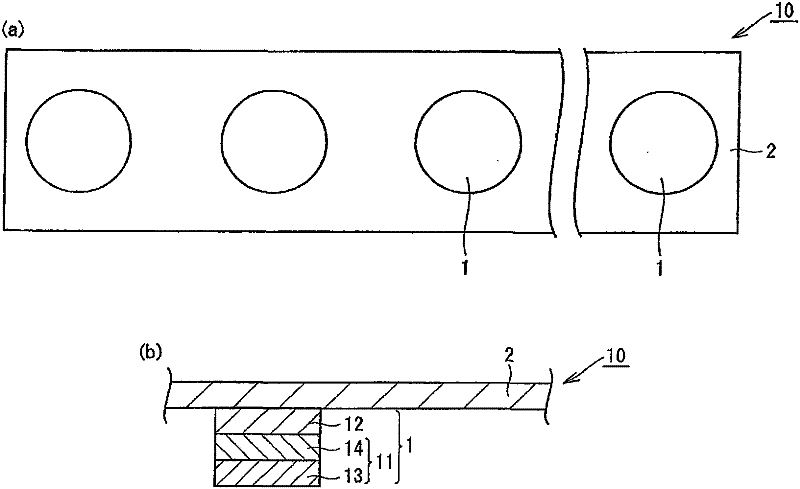
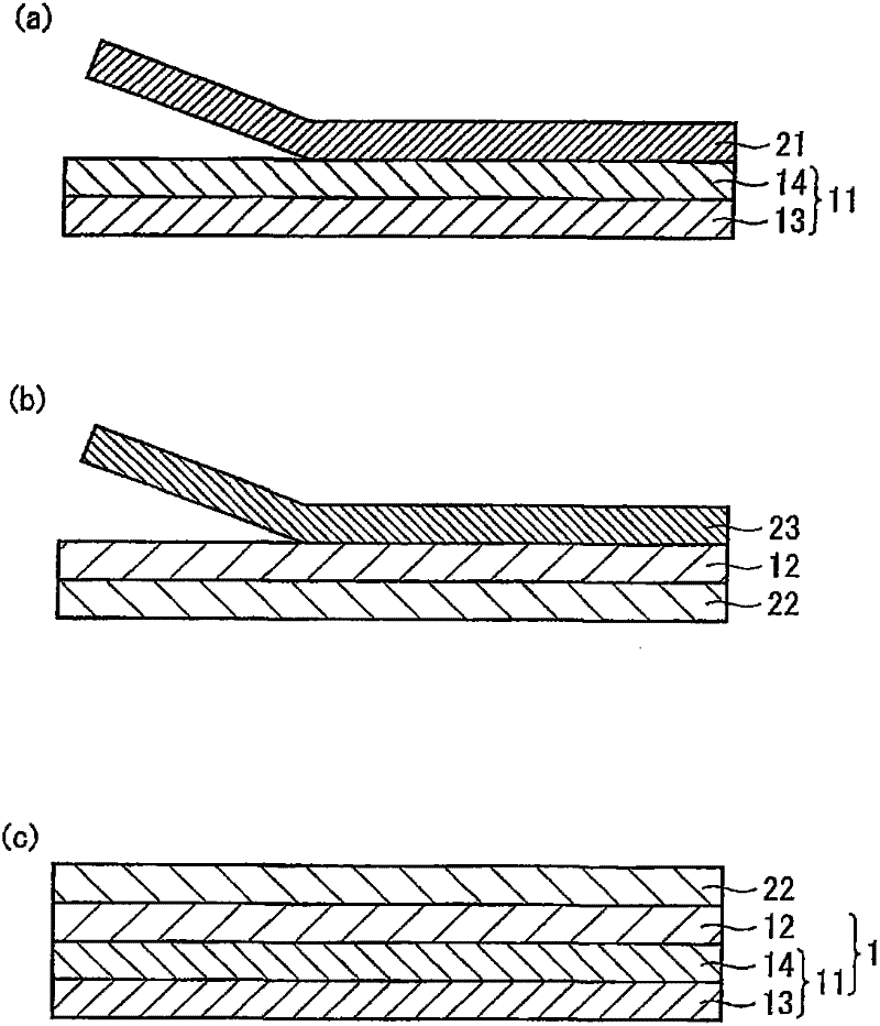
The present invention provides a film for a semiconductor device and the semiconductor device. The film for a semiconductor device is capable of suppressing the generation of a transfer mark on an adhesive film when a film for a semiconductor device, in which an adhesive film with a dicing sheet obtained by laminating an adhesive film onto a dicing film is laminated onto a cover film leaving a prescribed spacing, is wound up into a roll. It is a film for a semiconductor device in which an adhesive film with a dicing sheet obtained by laminating an adhesive film onto a dicing film is laminated onto a cover film leaving a prescribed spacing, wherein a ratio Ea / Eb of the tensile storage modulus Ea of the adhesive film at 23 DEG C. to the tensile storage modulus Eb of the cover film at 23 DEG C. is in a range of 0.001 to 50.

Description

technical field [0001] The present invention relates to a thin film for a semiconductor device and a semiconductor device manufactured using the thin film for a semiconductor device. Background technique [0002] Conventionally, in the manufacturing process of semiconductor devices, silver paste has been used to fix semiconductor chips to lead frames and electrode members. The fixing process is performed by applying a paste-like adhesive on a die pad of a lead frame, etc., mounting a semiconductor chip thereon, and curing the paste-like adhesive layer. [0003] However, the slurry adhesive has large variations in coating amount, coating shape, etc. due to its viscosity behavior, deterioration, and the like. As a result, the thickness of the paste-like adhesive formed is not uniform, so that the bonding strength of the semiconductor chip lacks reliability. That is, when the coating amount of the paste-like adhesive is insufficient, the adhesion strength between the semicond...

Claims


Application Information

Patent Timeline
Patent Type & Authority Applications(China)
IPC IPC(8): H01L21/00
CPCH01L21/67132H01L21/67092Y10T428/21Y10T428/31504Y10T428/31855C09J7/00H01L21/78
Inventor 天野康弘盛田美希
Owner NITTO DENKO CORP
Learn More