Process for making an embossed web
a technology of embossed webs and embossed edges, which is applied in the field of embossed web making processes, can solve the problems of inefficient vacuum forming process, high cost and inefficiency of hydroforming process, and limited amount of vacuum forming process,
- Summary
- Abstract
- Description
- Claims
- Application Information
AI Technical Summary
Problems solved by technology
Method used
Image
Examples
example 1
[0117]Embossed webs were produced using a compliant substrate 36 of 5.88 mm thick 40 A Gum Rubber and a forming structure 10 having about 486 apertures per square centimeter. The compliant substrate 36 had a Shore A hardness of about 40. The compliant substrate was in the form of a sheet 25.4 mm×25.4 mm square.
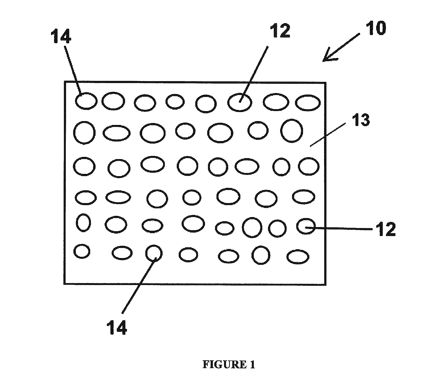
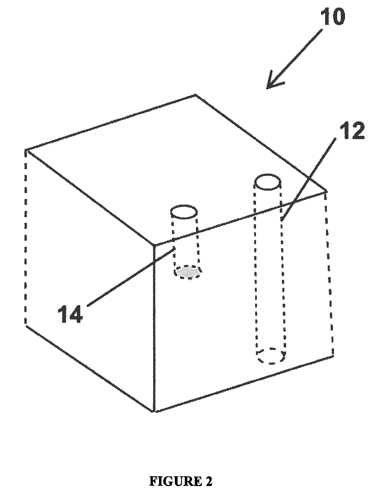
[0118]The forming structure had a thickness of about 2.25 mm. The apertures had a circular cross-section with an about 250 micron diameter at the top surface and a 2° taper from a top surface of the aperture into the depth of the aperture. The apertures had an edge-to-edge spacing of about 200 microns.
[0119]The precursor web 34 utilized was a polyethylene / polypropylene blend film obtained from RKW US, Inc. that was about 15 microns thick and had a basis weight of 14.2 grams per square meter (“gsm”).
[0120]The embossing process was performed using a high speed research press at room temperature. The high speed research press is described in detail in U.S. Patent Publication No. ...
example 2
[0123]Embossed webs were produced using a compliant substrate 36 of 3.28 mm thick 40 A Gum Rubber and a forming structure 10 having about 1550 apertures per square centimeter. The compliant substrate 36 had a Shore A hardness of about 40. The compliant substrate was in the form of a sheet 25.4 mm×25.4 mm square.
[0124]The forming structure had a thickness of about 1.02 mm. The apertures had a circular cross-section with an about 147 micron diameter at the top surface and a 2° taper from a top surface of the aperture into the depth of the aperture. The apertures had an edge-to-edge spacing of about 107 microns.
[0125]The precursor web 34 utilized was a polyethylene / polypropylene blend film obtained from RKW US, Inc. that was about 15 microns thick and had a basis weight of 14.2 grams per square meter (“gsm”).
[0126]The embossing process was performed using a high speed research press, as described in the preceding example. The press was operated to simulate compliant substrate and formi...
PUM
| Property | Measurement | Unit |
|---|---|---|
| melting point | aaaaa | aaaaa |
| width | aaaaa | aaaaa |
| depth | aaaaa | aaaaa |
Abstract
Description
Claims
Application Information


