Combined image sensor and display device

a combined image sensor and display device technology, applied in the field of combined image sensors and display devices, can solve the problems of reducing the aperture ratio of such a display, affecting the appearance of the display, so as to achieve the effect of improving the display aperture ratio and improving the appearan

Active Publication Date: 2010-09-16
SHARP KK
View PDF34 Cites 53 Cited by
  • Summary
  • Abstract
  • Description
  • Claims
  • Application Information

AI Technical Summary

Benefits of technology

[0013]The polarity of the photocurrent may be such as to reduce the absolute value of the voltage at the control electrode during the sensing phase.
[0014]It is thus possible to provide a device having an improved display aperture ratio while combining the functions of a display and an image sensor. A greater portion of the device area may be used for display purposes, for example to provide a brighter display of improved appearance. Such a device may be manufactured using thin-film semiconductor process or silicon-on-insulator process technology.

Problems solved by technology

However, the presence of the image sensing function within the pixels reduces the aperture ratio of such a display as compared with a display in which no image sensing function is provided.
However, the size of such an array is limited by the time needed to integrate each row sequentially and the output signals suffer from a relatively large degree of noise associated with fluctuations in the column current during integration.
Thus, in the absence of the integration capacitance, the pixel discharge rate would be too high for practical use.

Method used


Image

  • Combined image sensor and display device
  • Combined image sensor and display device
  • Combined image sensor and display device

Examples


Embodiment Construction

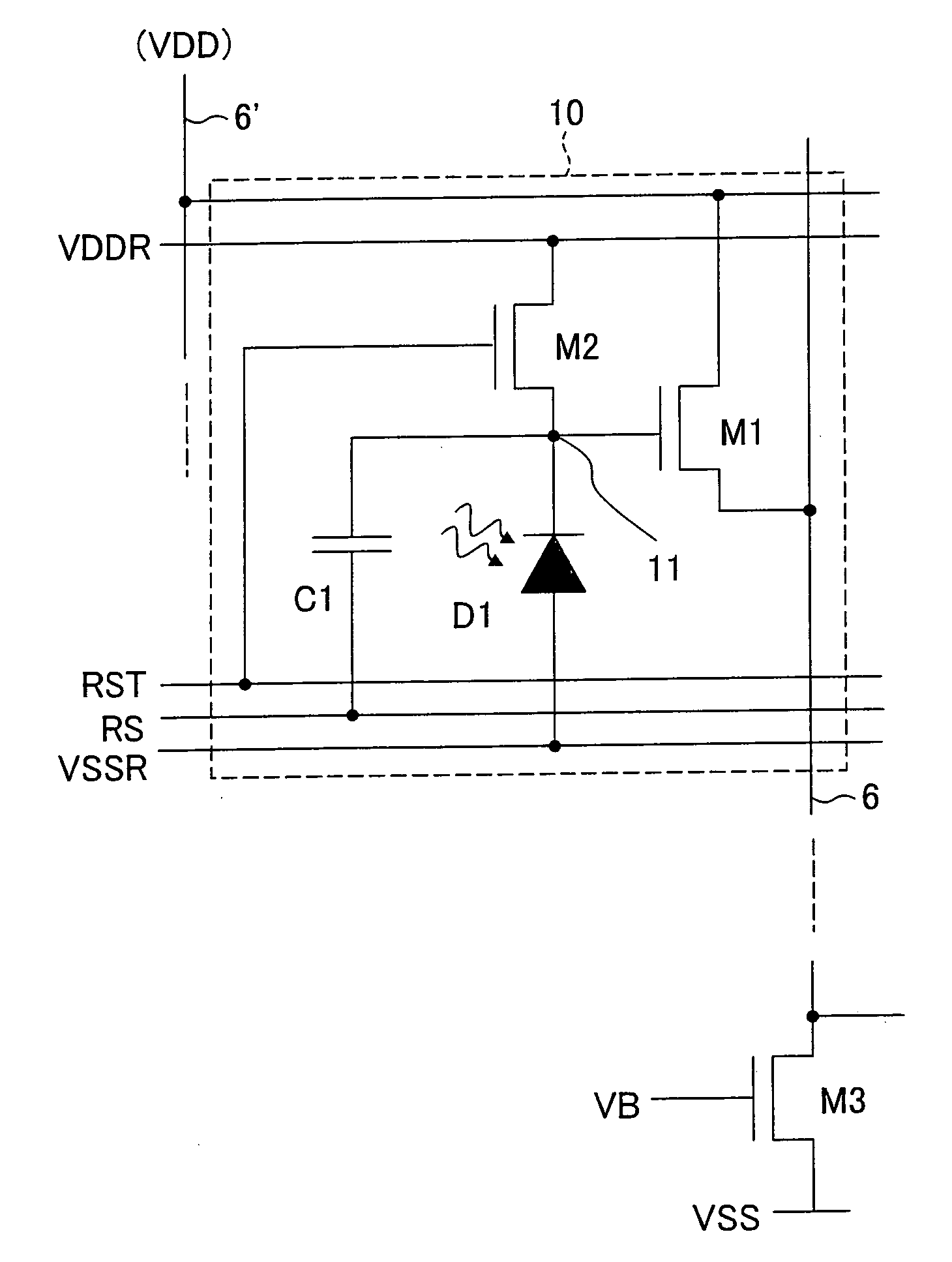
[0043]A combined image sensor and display device comprises an array of rows and columns of sensor elements, each of which is as illustrated at 10 in FIG. 5. The sensor elements 10 together with addressing and output circuits are integrated on a common substrate, for example using thin-film transistor or silicon-on-insulator techniques. The sensor comprises an active matrix device, which is combined with an active matrix display of the liquid crystal type as described hereinafter.

[0044]The sensor element 10 comprises a photodetecting element embodied as a lateral thin-film photodiode D1, whose anode is connected to a line VSSR common to all the sensor elements of the row and carrying a photodiode anode potential VSSR. The cathode of the photodiode is connected to an integrating node 11, which is connected to the first electrode or plate of an integrating capacitor C1. The second electrode or plate of the capacitor C1 is connected to a row select line RS, which is common to the sensor...


PUM


Abstract

A combined image sensor and display device comprises an array of device elements (18), each of which comprises a display pixel (M4, C2, CLC). The display pixels have data inputs connected to column data lines (SL, 6,6′). The array includes sensor elements (10), each comprising a transistor (M1), an integrating capacitor (C1) and a photodiode (D1) connected together to an integrating node (11). The transistor (M1) is connected between column data lines (6,6′). The capacitor (C1) is connected to a control input (RS) which receives a first voltage during a sensing phase for switching off the transistor (M1) and a second voltage during a reading phase for enabling the transistor (M1).

Description

TECHNICAL FIELD[0001]The present invention relates to a combined image sensor and display device.BACKGROUND ART[0002]There is a desire to fabricate an image sensor in a thin-film polysilicon process which is compatible with that used in the manufacture of thin-film transistor substrates for active matrix liquid crystal displays (AMLCDs). By using such a fabrication process, such an image sensor may be monolithically integrated within an AMLCD in order to provide, for example, an input function for detecting a touch or pen input. In such an arrangement, each pixel may include both image sensing and displaying elements to provide similar spatial resolutions of image sensing and display. However, the presence of the image sensing function within the pixels reduces the aperture ratio of such a display as compared with a display in which no image sensing function is provided.[0003]Several types of semiconductor image sensors exist, including those based on charge-coupled device (CCD) tec...

Claims


Application Information

Patent Timeline
Patent Type & Authority Applications(United States)
IPC IPC(8): G06F3/038G06F3/041G09G5/00H04N5/335
CPCG06F3/0412G06F3/042G09G3/3648H04N5/335H01L27/14609H01L27/14643G09G2360/142H04N25/00H01L27/14806H04N3/1525G09G3/36G02F1/1368H01L27/146
Inventor BROWN, CHRISTOPHER JAMES
Owner SHARP KK
Why Eureka
Try Eureka