Supercharge Your Innovation With Domain-Expert AI Agents!

Package substrate

a technology of packaging substrate and substrate, applied in the direction of fixed capacitor details, association of printed circuit non-printed electrical components, electrical apparatus contruction details, etc., can solve the problems of unlikely to occur and reduce reliability, and achieve the effect of reducing thickness and siz

Active Publication Date: 2010-09-16
MURATA MFG CO LTD
View PDF12 Cites 6 Cited by
  • Summary
  • Abstract
  • Description
  • Claims
  • Application Information

AI Technical Summary

Benefits of technology

The present invention provides a package substrate that does not require embedding an electronic component in the main package, which reduces the size of the substrate and improves reliability. The package substrate includes a main package body and a sub-package. The main package body has a first bonding material on its second principal surface, while the sub-package has a first pad conductor and a second pad conductor that function as input and output paths for the internal circuit. The sub-package can be embedded within the recess of the main package body, and the thickness direction dimension of the sub-package is equal or substantially equal to or less than the thickness direction dimension of the first bonding material. This reduces the overall size and thickness of the package substrate. The package substrate also includes a main package body and a sub-package that are electrically connected through the first bonding material. The reliability of the electrical connection is improved, and the size and thickness of the package substrate are reduced.

Problems solved by technology

In addition, because an independent electronic component is not embedded in the main package body, a decrease in reliability that is caused due to an undesirable gap between the main package body and the electronic component is unlikely to occur.

Method used


Image

  • Package substrate
  • Package substrate
  • Package substrate

Examples


Embodiment Construction

[0041]Hereinafter, specific preferred embodiments of the invention will be described with reference to the accompanying drawings to clarify the invention.

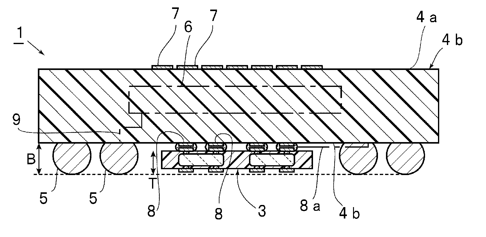
[0042]FIG. 1 is a front view of a package substrate according to a first preferred embodiment of the present invention.

[0043]The package substrate 1 includes a main package 2 and a sub-package 3. Specifically, the main package 2 preferably has a substantially rectangular-parallelepiped-shaped main package body 4, for example. The main package body 4 includes a first principal surface 4a and a second principal surface 4b that are opposed to each other. On the second principal surface 4b, a plurality of first bonding materials 5 is provided.

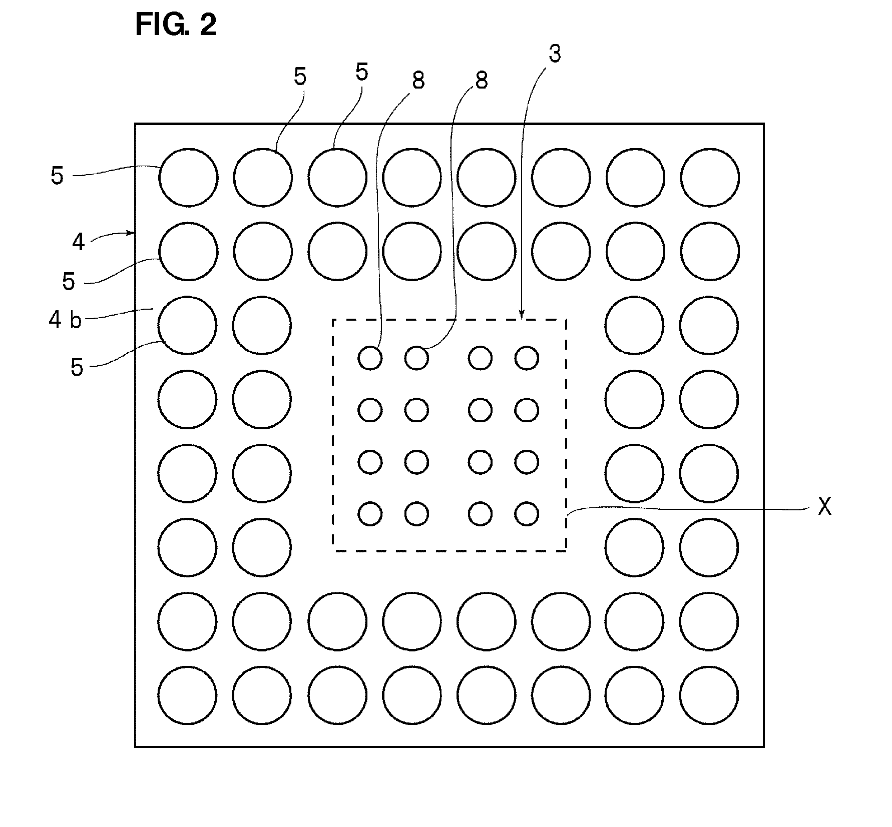
[0044]FIG. 2 is a bottom view of the package substrate 1. The plurality of first bonding materials 5 are provided on the second principal surface 4b of the main package body 4 so as to preferably be substantially in the shape of a rectangular frame, for example. The plurality of first bonding mate...


PUM


Abstract

A package substrate includes a main package body including a first principal surface on which an IC is mounted, and a second principal surface, opposed to the first principal surface, on which first bonding materials for mounting are provided. An internal circuit is provided within the main package body and connected to the first bonding materials. A sub-package is arranged on the second principal surface and includes electronic components embedded therein. A thickness direction dimension being the distance from the second principal surface to a portion of the sub-package most distant from the second principal surface, is not more than a thickness direction dimension being the distance from the second principal surface to an edge of the first bonding material at the second principal surface.

Description

BACKGROUND OF THE INVENTION[0001]1. Field of the Invention[0002]The present invention relates to a package substrate used for a package for an electronic component, and more particularly, to a package substrate having an internal circuit and a structure in which a plurality of independent electronic components electrically connected to the internal circuit are included.[0003]2. Description of the Related Art[0004]Recently, cellular phones and personal computers use MPUs having increased clock frequencies. Thus, noise having many harmonics is likely to be superimposed in power supply lines for the MPUs.[0005]In order to prevent the above adverse effect caused by the noise, typically a decoupling capacitor is often connected between a power supply line and a ground. The decoupling capacitor is a necessary element of a power supply circuit because the decoupling capacitor also suppresses a transient phenomenon of a power supply system.[0006]In the related art, the decoupling capacitor ...

Claims


Application Information

Patent Timeline
Patent Type & Authority Applications(United States)
IPC IPC(8): H05K7/02
CPCH01G4/232H01G4/40H01L23/49816H01L23/49838H01L23/50H05K7/026H01L2224/16H01L2924/01046H01L2924/01078H01L2924/01079H01L2924/15311H01L23/5389H01L2924/15159H01L2924/19106H01L2224/05026H01L2224/05568H01L2224/05001H01L2924/00014H01L2224/05599H01L2224/05099
Inventor MAEDA, ATSUYOSHIITO, SHINGONODA, SATORU
Owner MURATA MFG CO LTD
Features
  • R&D
  • Intellectual Property
  • Life Sciences
  • Materials
  • Tech Scout
  • Unparalleled Data Quality
  • Higher Quality Content
  • 60% Fewer Hallucinations
Learn More