Nonvolatile semiconductor memory device and method of operating the same

Active Publication Date: 2010-09-23
KIOXIA CORP
View PDF2 Cites 2 Cited by
  • Summary
  • Abstract
  • Description
  • Claims
  • Application Information

AI Technical Summary

Benefits of technology

[0009]In accordance with a first aspect of the present invention, a nonvolatile semiconductor memory device comprises: a memory cell array having a plurality of memory cells arranged therein, each of the memory cells capable of storing multiple bits of information including multiple pages of information and is allocated to a plurality of threshold voltage distributions; and a control circuit configured to write information to a memory cell by applying a voltage to a bit line and a word line to change a threshold voltage of the memory cell, during writing of information to a plurality of the memory cells connected to an identical word line, the control circuit being configured to apply, to each of the bit lines corresponding to the plurality of the memory cells, any one of voltages that differ from one another according to the multiple bits of information to be written.
[0010]In accordance with a second aspect of the present invention, a nonvolatile semiconductor memory device comprises: a memory cell array having a plurality of memory cells arranged therein, each of the memory cells capable of storing multiple bits of information including multiple pages of information and is allocated to a plurality of threshold voltage distributions; and a control circuit configured to write information to a memory cell by applying a voltage to a bit line and a word line to change a threshold voltage of the memory cell, the control circuit comprising: a data latch circuit configured to retain data of one page out of the multiple pages as information to be written to the memory cells; an arithmetic circuit configured to perform a logical operation on the multiple pages of information retained in the data latch circuit; a sense amplifier circuit configured to contro

Problems solved by technology

This kind of multi-value storage NAND flash memory has the problem that the number of applications (number of step-ups) of the write voltage Vpgm applied to the control gate of the memory cell differs according to the data to be stored, resulting in a lengthening of write time.
If, to reduce the number of applications, the initial value Vpgmi of the write voltage Vpgm is increased or a step-up width is increased, there is a risk that an erroneous write occurs in the memory cells where the low threshold voltage distribution A is to be written.
The initial value and step-up width must therefore beset in line with the case where data of the low threshold voltage distribution is written, and this results in a lengthening of the write time.

Method used


Image

  • Nonvolatile semiconductor memory device and method of operating the same
  • Nonvolatile semiconductor memory device and method of operating the same
  • Nonvolatile semiconductor memory device and method of operating the same

Examples


first embodiment

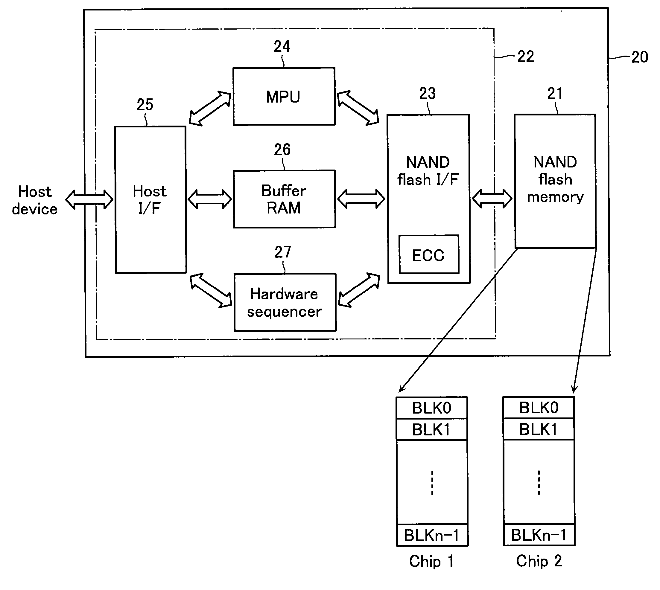
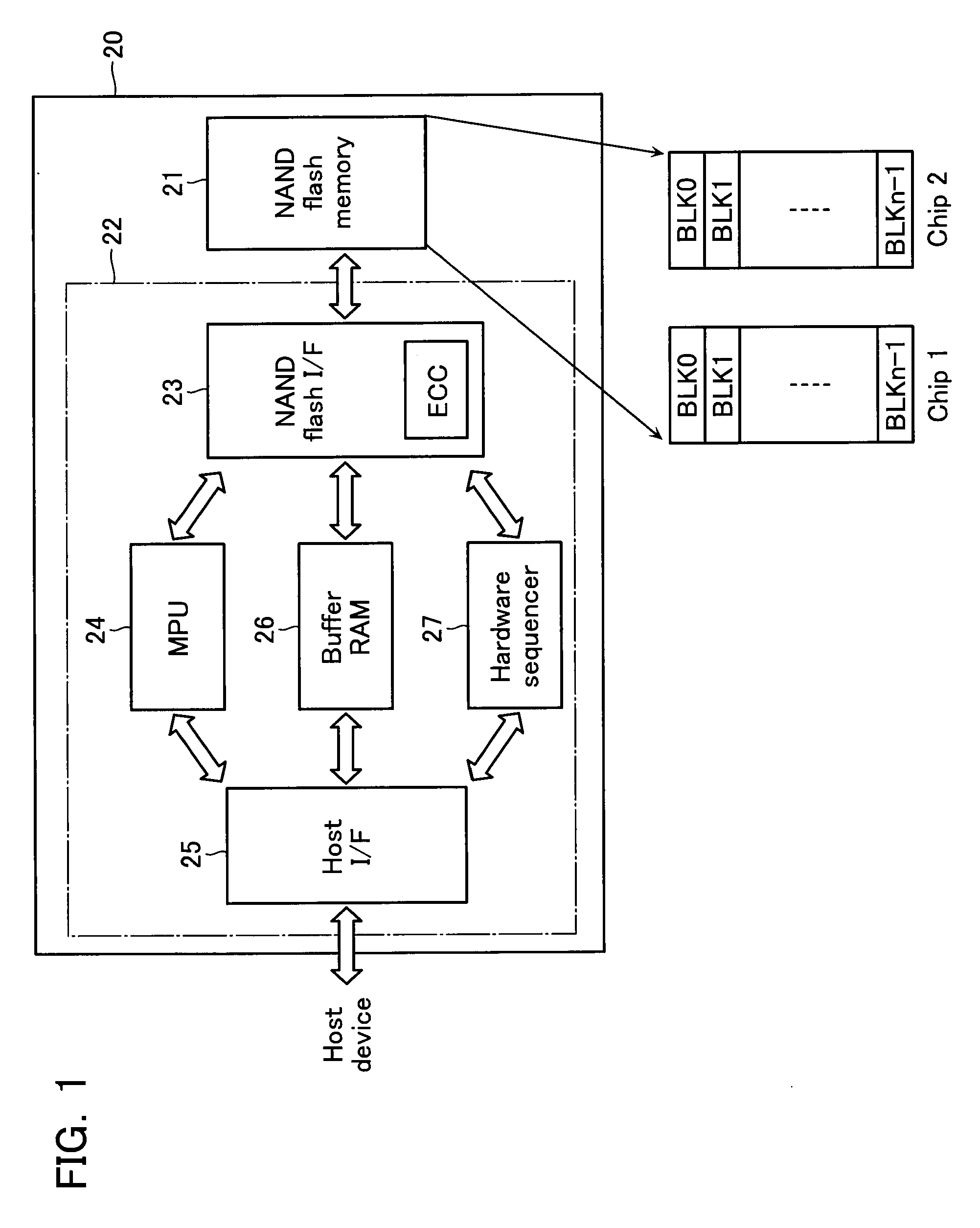
[0026]First, a nonvolatile semiconductor memory device in accordance with a first embodiment of the present invention is described with reference to FIG. 1 and so on.

[0027][Overall Configuration of System]

[0028]FIG. 1 is a block diagram showing an overall configuration of a memory card 20, which represents the nonvolatile semiconductor memory device in accordance with the first embodiment. The memory card 20 configures modules with a NAND flash memory 21 and a memory controller 22 that controls read / write operations of the NAND flash memory 21. The NAND flash memory chip 21 may be a plurality of memory chips. Although FIG. 1 shows two memory chips, i.e., chip 1 and chip 2, they are also controlled by the single memory controller 22. The memory controller 22 is a one-chip controller that includes a NAND flash interface 23 for transferring data to and from the NAND flash memory 21, an MPU 24 for controlling, not only data transfer, but also entire operations in the memory card, a host...

second embodiment

[0067]Next, a second embodiment of the present invention is described with reference to FIGS. 12 and 13.

[0068]The present embodiment is substantially similar to the first embodiment regarding overall configuration and so on of the nonvolatile semiconductor memory device (FIGS. 1-9). However, in the present embodiment, a procedure (method) for control of the write data inputted to the data latch circuit and the bit line voltage based on this write data differs from that of the first embodiment.

[0069]FIG. 12 is a flowchart showing the procedure for control of the bit line voltage in the nonvolatile semiconductor memory device in accordance with the present embodiment. FIG. 13 is a view showing a logical operation in an arithmetic circuit and data retained in a data latch circuit in the nonvolatile semiconductor memory device in accordance with the present embodiment. FIG. 13 shows the correspondence between the threshold voltage distributions Er and A-C, and data retained in the sense...


PUM


Abstract

A nonvolatile semiconductor memory device comprises: a memory cell array having a plurality of memory cells arranged therein, each of the memory cells capable of storing multiple bits of information including multiple pages of information and is allocated to a plurality of threshold voltage distributions; and a control circuit configured to write information to a memory cell by applying a voltage to a bit line and a word line to change a threshold voltage of the memory cell. During writing of information to a plurality of the memory cells connected to an identical word line, the control circuit is configured to apply, to each of the bit lines corresponding to the plurality of the memory cells, any one of voltages that differ from one another according to the multiple bits of information to be written.

Description

CROSS REFERENCE TO RELATED APPLICATIONS[0001]This application is based upon and claims the benefit of priority from prior Japanese Patent Application No. 2009-63883, filed on Mar. 17, 2009, the entire contents of which are incorporated herein by reference.BACKGROUND OF THE INVENTION[0002]1. Field of the Invention[0003]The present invention relates to a nonvolatile semiconductor memory device, in particular, to a nonvolatile semiconductor memory device capable of storing multiple bits in one memory cell, and to a method of operating the same.[0004]2. Description of the Related Art[0005]NAND flash memory is known as one of nonvolatile semiconductor memory devices. This NAND flash memory has a memory cell array including a plurality of NAND cell units. Each NAND cell unit is configured by a plurality of memory cells connected in series and two select transistors connected to both ends thereof.[0006]Each memory cell stores, in an erase state, data “1” having a negative threshold voltage...

Claims


Application Information

Patent Timeline
IPC IPC(8): G11C16/04G11C7/10
CPCG11C16/3404G11C11/5628
Inventor KOMAI, HIROMITSU
Owner KIOXIA CORP
Why Eureka
Try Eureka