Image processing device, image processing method, and image processing program

a technology of image processing and aberration distortion, applied in the field of correction of aberration distortion, can solve the problems of long processing time, high computational load of high-order calculations, and unfavorable efficiency, and achieve the effect of high precision, easy computable, and no memory space and processing time increas

Active Publication Date: 2010-09-30
INTEL CORP
View PDF2 Cites 16 Cited by
  • Summary
  • Abstract
  • Description
  • Claims
  • Application Information

AI Technical Summary

Benefits of technology

[0056]In the image processing device the image processing method, and and the image processing program according to the present invention it is determined for predetermined pixel positions in an output image, how a aberration distortion can be compensated. In pixel positions in the output image other than the predetermined pixel position a high order polynomial is used to calculate the sampling position in the input image. The sampling position in the input image is computed by an interpolating calculation from the sampling positions corresponding to those predetermined output pixels located near this pixel. By sampling the pixel value of said input image in this way, distortion of the aberration distortion resulting from an image formation optical system, etc. can be compensated with high precision, without increasing memory space and processing time.
[0057]In the embodiment of the image processing device, the image processing method, and the image processing program of the invention wherein the sampling position is computed with bilinear interpolation as the interpolating calculation, the sampling positions corresponding to pixel positions other than the predetermined pixel positions in the output image, are relatively easily computable. This enables a faster processing time and a lower power consumption than would be the case if the sampling position were calculated by a high order polynomial for all output pixels.
[0058]In the embodiment of the image processing device, the image processing method, and the image processing program wherein the sampling position is computed by cubic interpolation (also denoted as third order interpolation) as the interpolating calculation for those pixel positions other than the predetermined pix

Problems solved by technology

Accordingly it is a problem that storing the correction value for the sampling position in the input image in a memory for each pixel of the output image, requires a large memory capacity for storing the correction values and is unfavorable for the efficiency.
Accordingly, the method of matching all pixels of an output image by computing the sampling position of an input image using a high order polynomial, as disclo

Method used


Image

  • Image processing device, image processing method, and image processing program
  • Image processing device, image processing method, and image processing program
  • Image processing device, image processing method, and image processing program

Examples


first embodiment

[0116]Next, the image processing device of this invention and an image processing method, as well as an image processing program are described with reference to the drawings

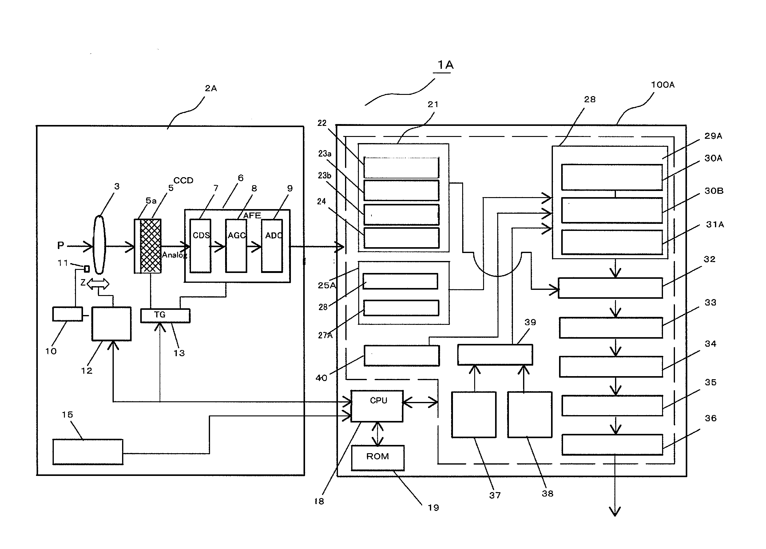
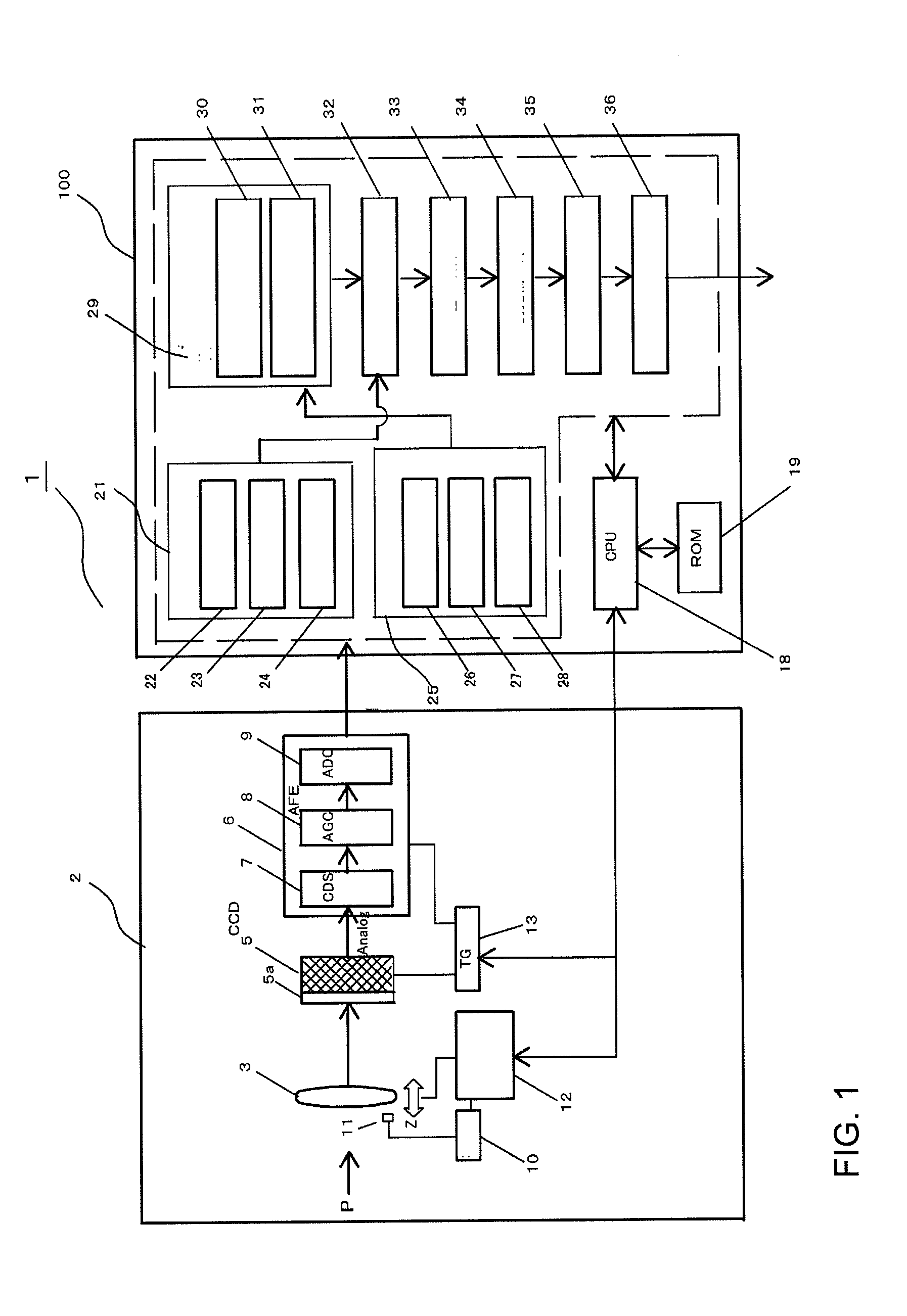
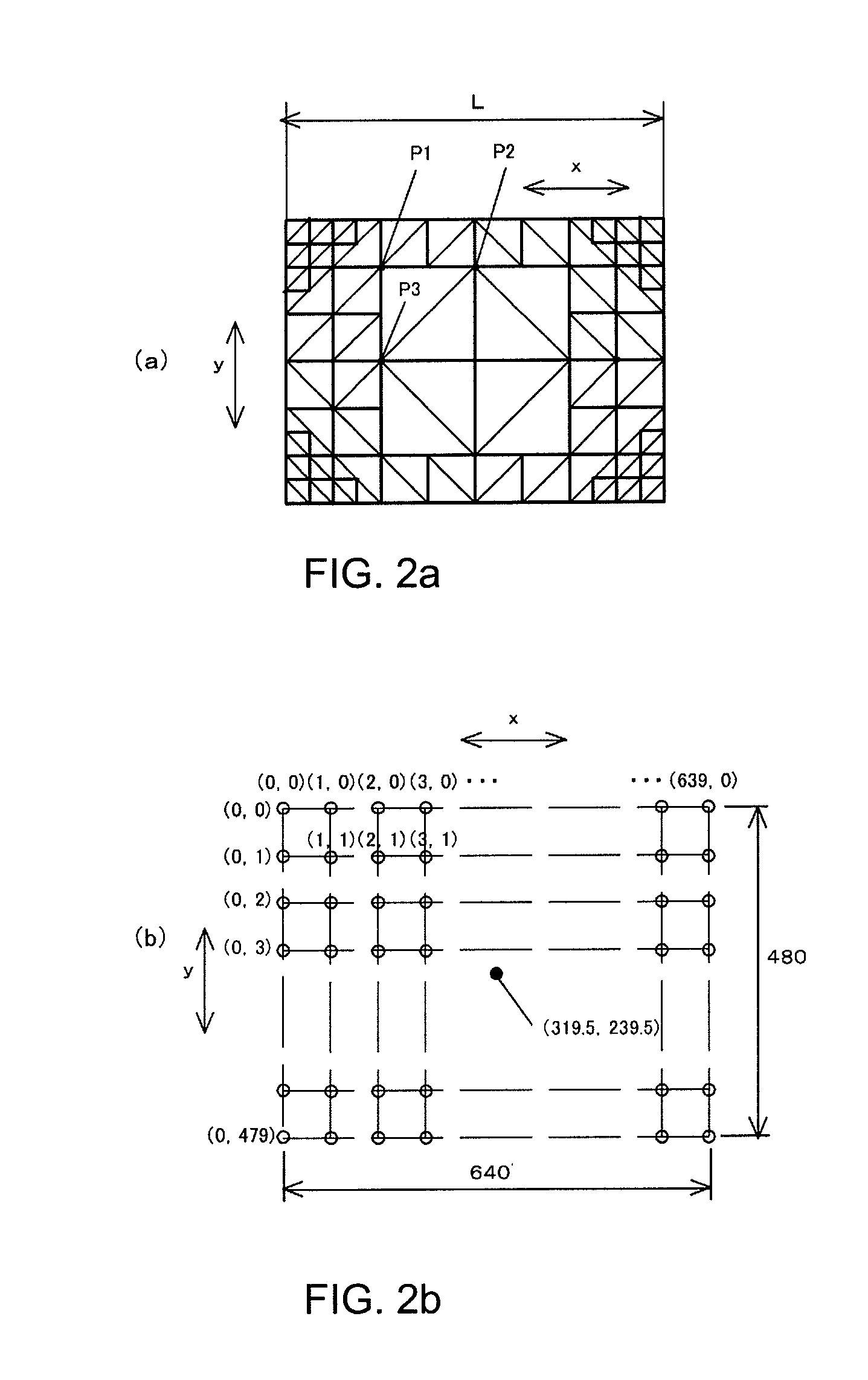
[0117]FIG. 1 is a block diagram showing the composition of the imaging device 1 of one example to which the image processing device of this invention and the image processing method, and the image processing program may be applied. FIG. 2(a) is an explanatory view of a starting point coordinate set. FIG. 2a shows an example of block division of the output image, and FIG. 2(b) shows the output image of the first embodiment.

[0118]FIG. 3 illustrates a function of the color plane decomposition unit and a color generation unit in the first embodiment. FIG. 3a shows the color mosaic image of a Bayer array outputted by the imaging optical system 2. FIGS. 3b, 3c and 3d respectively show the R plane, G plane, and B plane arrangement generated by the color plane decomposition and Figure (e) illustrates an interpolation cal...

second embodiment

[0180]FIG. 7 shows the generation of uv vertex-coordinates in the output image in the second embodiment and an explanatory view of, and FIG. 8 shows an example of a lookup table comprising aberration coefficients used for image processing in this example.

[0181]FIG. 9 illustrates operation of a color plane decomposition unit and a color generation unit in the second embodiment. FIG. 9(a) shows a color mosaic image of a Bayer array outputted by the imaging optical system 2. FIGS. 9(b), (c), (d), and (e) respectively show the R plane, the Gr plane, the Gb plane, and the B plane as generated by the color plane decomposition unit, respectively and Figure (f) shows carrying out interpolation calculation of the pixel value in sampling coordinates.

[0182]FIG. 10 is a figure showing an image processing procedure in an image processing program in this embodiment.

[0183]Parts of the imaging device 1A in this second embodiment that correspond to those of imaging device 1 according to the first em...


PUM


Abstract

An image processing device, an image processing method, and an image processing program by which deformation such as distortion caused by an imaging optical system can be corrected with high precision without increase in memory capacity and processing time. The image processing device comprises a vertex sampling coordinate computing section (30) for computing a sampling position on an input image by a high-order expression so as to cancel out distortion at the position of a predetermined pixel of an output image, a sampling coordinate interpolation computing section (31) for interpolating the sampling position on the input image, at the position of a pixel other than the position of the predetermined pixel of the output image, from a sampling position of a predetermined output pixel located near the pixel, and a sampling unit (32) for sampling a pixel value of the input image at the sampling position computed via the vertex sampling coordinate computing section (30) and the sampling coordinate interpolation computing section (31).

Description

BACKGROUND OF THE INVENTION[0001]1. Field of the Invention[0002]The present invention relates to correction of aberration distortions, in particular by image processing, in an image formation optical system, such as a digital camera provided with the electronic imaging optical system.[0003]2. Background of the Invention[0004]In the imaging system of a digital camera image formation is conventionally carried out by an imaging lens that projects an object image onto an image sensor. The image sensor has a plurality of optoelectric transducers arranged in a matrix form that provide for a photoelectric conversion of the object image projected by the lens. An image processing device using an image processing method then generates an output image using the picture signal provided by the image sensor.[0005]In current digital camera's, the pixel positions of the output image, match with those of the picture obtained from the image sensor (also denoted as input image). Each pixel signal samp...

Claims


Application Information

Patent Timeline
IPC IPC(8): G06K9/40H04N5/232
CPCH04N9/045H04N5/3572H04N23/843H04N25/134H04N23/60H04N25/61H04N23/10
Inventor SAWADA, YASUHIRO
Owner INTEL CORP
Why Eureka
Try Eureka