Semiconductor integrated circuit and method for manufacturing semiconductor integrated circuit

a technology of integrated circuits and semiconductors, applied in the direction of generating/distributing signals, pulse techniques, instruments, etc., can solve the problems of all transistors can be advanced-deteriorated, etc., to achieve the effect of suppressing the increase of wiring, increasing no processing time, and not increasing processing time and wiring

Inactive Publication Date: 2006-09-07
PANASONIC CORP
View PDF14 Cites 3 Cited by
  • Summary
  • Abstract
  • Description
  • Claims
  • Application Information

AI Technical Summary

Benefits of technology

[0016] In the semiconductor integrated circuit and the semiconductor integrated circuit manufacturing method of the present invention, propagation of the clock signal in the clock control signal output terminal of the clock control circuit is controlled by inputting the burn-in control signal to the burn-in control signal input terminal of the clock control circuit. With this, all the transistors can be advance-deteriorated. Also, one-time processing allows the transistors to be advance-deteriorated, thus increasing no processing time. Furthermore, the burn-in control signal input terminal and the wiring are added only to the clock control circuit, so that an increase of the wiring can be suppressed.
[0017] Moreover, by changing the signal-fixed direction, all the transistors can be advance-deteriorated without increasing the processing time and the wirings. Also, one-time processing allows the transistors to be advance-deteriorated, thus increasing no processing time.
[0018] Furthermore, with the semiconductor integrated circuit and the semiconductor integrated circuit manufacturing method of the present invention, all the transistors in the clock circuit that supplies and controls the clock signals can be advance-deteriorated without increasing the processing time and the wirings.

Problems solved by technology

With this, all the transistors can be advance-deteriorated.
Also, one-time processing allows the transistors to be advance-deteriorated, thus increasing no processing time.

Method used


Image

  • Semiconductor integrated circuit and method for manufacturing semiconductor integrated circuit
  • Semiconductor integrated circuit and method for manufacturing semiconductor integrated circuit
  • Semiconductor integrated circuit and method for manufacturing semiconductor integrated circuit

Examples


first embodiment

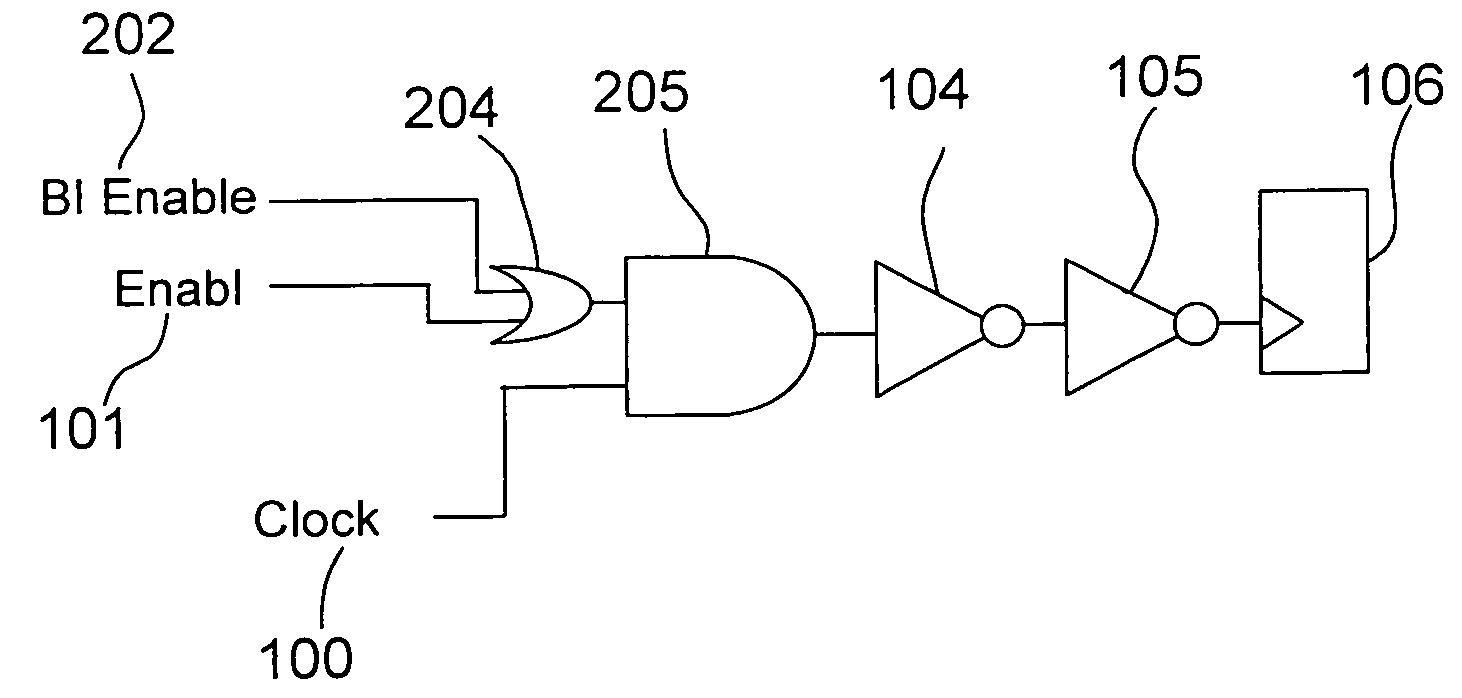
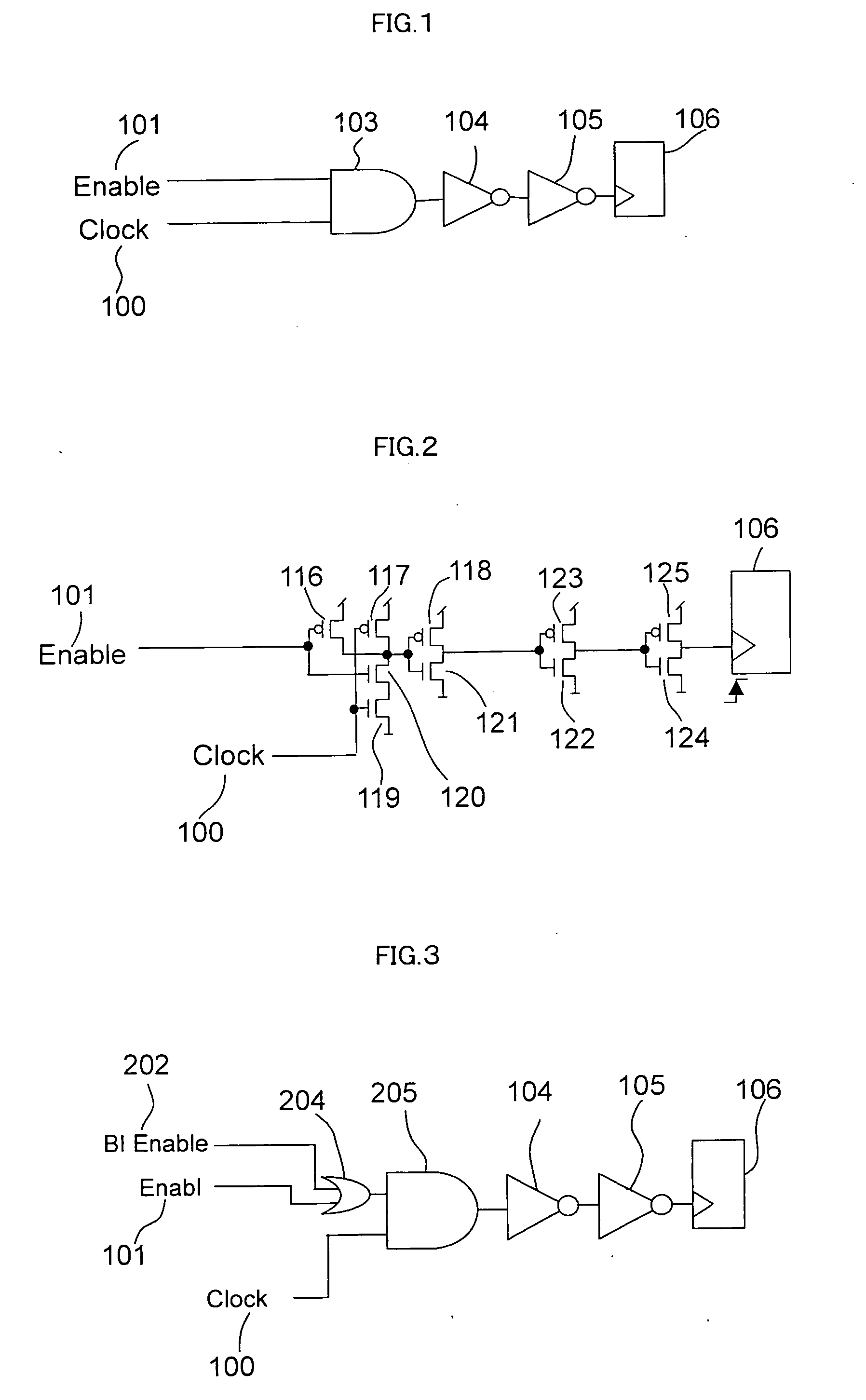
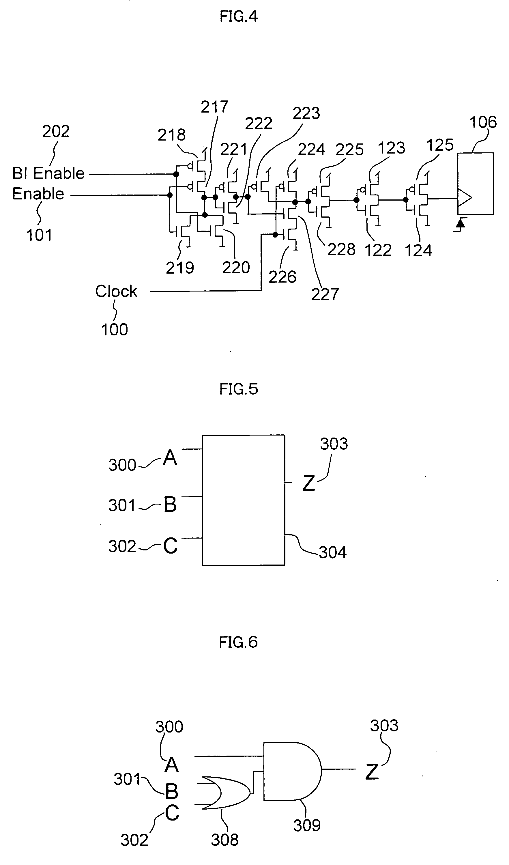
[0053] A first embodiment of the present invention will be described by referring to FIG. 1-FIG. 9. FIG. 1 is a block diagram for showing a typical example of a clock circuit that comprises clock control circuits. FIG. 2 is a block diagram (circuit diagram) of conventional transistors which achieve the clock control circuit of FIG. 1. FIG. 3 is a block diagram for showing the structure of the clock circuit according to the embodiment, which comprises the clock control circuits with BI control signal input terminal. FIG. 4 is a block diagram (circuit diagram) of transistors according to the embodiment, which achieve the clock control circuit of FIG. 3. FIG. 5-FIG. 9 are illustrations for describing the clock control circuit with BI control signal input terminal according to the embodiment.

[0054] In FIG. 1, reference numeral 100 is a clock signal, 101 is a clock control signal, 103 is an AND circuit, 104, 105 are inverter circuits, 106 is a rise signal action flip-flop.

[0055]FIG. 2 ...

second embodiment

[0078] A second embodiment of the present invention will be described by referring to FIG. 10-FIG. 18. The same reference numerals are applied to the same structural elements as those of the first embodiment, and the description thereof will be omitted. FIG. 10 is a block diagram for showing an example the clock circuit that comprises a clock control circuit with BI control signal input terminal. FIG. 11-FIG. 14 are illustration for describing the clock control circuit with BI control signal input / output terminal of this embodiment. FIG. 15 is a block diagram showing another example of the clock circuit that comprises a clock control circuit with BI control signal input / output terminal. FIG. 16 and FIG. 17 are flowcharts for showing the procedures of a chain-type connecting method. FIG. 18 is a block diagram for showing a modification of the clock circuit of the embodiment, which comprises a clock control circuit with BI control signal input / output terminal.

[0079] In FIG. 10, refer...

third embodiment

[0106] A third embodiment of the present invention will be described by referring to FIG. 19 and FIG. 20. FIG. 19 and FIG. 20 are flowcharts for describing a manufacturing method of the clock circuit that comprises a control circuit with BI control signal in a part thereof.

[0107] In FIG. 19, reference numeral 800 is a CTS step, 801 is a toggle-rate measuring step, 802 is a replacing-target clock control circuit judging step, 803 is a clock control circuit replacing step, and 804 is a burn-in step. In FIG. 20, reference numeral 805 is a wiring step, 806 is a toggle-rate measuring step, 807 is a replacing-target clock control circuit judging step, 808 is a clock control circuit replacing step, and 809 is a burn-in step.

[0108] The manufacturing method illustrated in FIG. 19 will be described. For designing the clock circuit shown in FIG. 10, in order to reduce the clock-signal reaching-time difference (referred to as clock skew hereinafter) to the flip-flops, there requires clock tre...


PUM


Abstract

The semiconductor integrated circuit of the present invention comprises a clock circuit for generating a clock signal. The clock circuit comprises a clock control circuit for controlling propagation of the clock signal. The clock control circuit comprises a burn-in control signal input terminal for inputting a burn-in control signal that controls operation state of the clock circuit when performing burn-in processing, and a clock control signal output terminal for outputting the clock signal. The clock control circuit controls propagation of the clock signal outputted from the clock control signal output terminal based on the burn-in control signal inputted to the burn-in control signal input terminal.

Description

BACKGROUND OF THE INVENTION [0001] 1. Field of the Invention [0002] The present invention relates to a semiconductor integrated circuit that supplies and controls clock signals and to a method for manufacturing the semiconductor integrated circuit. [0003] 2. Description of the Related Art [0004] Most of semiconductor integrated circuits containing logic circuits operate by synchronizing with clock signals supplied from outside or clock signals generated inside thereof based on signals supplied form outside. In general, a semiconductor integrated circuit comprises a plurality of flip-flops and a circuit for (referred to as a clock circuit hereinafter) which generates clock signals to be supplied to each flip-flop based on supplied clock signals. In order for the semiconductor integrated circuit to operate properly, it is necessary to supply the clock signals properly to each flip-flop. [0005] Further, in order to reduce power consumption of the semiconductor integrated circuit, it is...

Claims


Application Information

Patent Timeline
Patent Type & Authority Applications(United States)
IPC IPC(8): G06F1/04H03K3/00
CPCG01R31/2856
Inventor MATSUMURA, YOICHIOHASHI, TAKAKOKIMURA, FUMIHIROMUKAI, KIYOHITOITOU, MASANORI
Owner PANASONIC CORP
Why Eureka
Try Eureka