High-Frequency Wiring Board and High-Frequency Module That Uses the High-Frequency Wiring Board

a high-frequency wiring and high-frequency module technology, applied in the direction of electrical apparatus, coupling devices, semiconductor devices, etc., can solve the problems of inability to provide a solution for related art, signal reflection tends to occur increasingly, mismatching tends to occur in the vicinity, etc., to achieve the effect of improving the reflection characteristics

Inactive Publication Date: 2010-10-07
NEC CORP
View PDF3 Cites 18 Cited by
  • Summary
  • Abstract
  • Description
  • Claims
  • Application Information

AI Technical Summary

Benefits of technology

[0018]It is an object of the present invention to provide a high-frequency signal line connection construction for solving the above-described problems. One example of this object is to provide a construction that enables an improvement of reflection characteristics from a low-frequency region to a high-frequency region in a high-frequency wiring board equipped with different types of lines that are formed on different layers and that are interconnected.

Problems solved by technology

However, when different types of line constructions formed on different layers are connected together, as with first high-frequency transmission lines and second high-frequency transmission lines, mismatching tends to occur in the vicinity of the connection portions, and as a result, signal reflection tends to occur increasingly as the frequency increases.
However, it was found that the related art could not provide a solution to the problem in which the reflection characteristics deteriorate as the transmission signal progresses from low frequencies to higher frequencies.

Method used


Image

  • High-Frequency Wiring Board and High-Frequency Module That Uses the High-Frequency Wiring Board
  • High-Frequency Wiring Board and High-Frequency Module That Uses the High-Frequency Wiring Board
  • High-Frequency Wiring Board and High-Frequency Module That Uses the High-Frequency Wiring Board

Examples


first embodiment

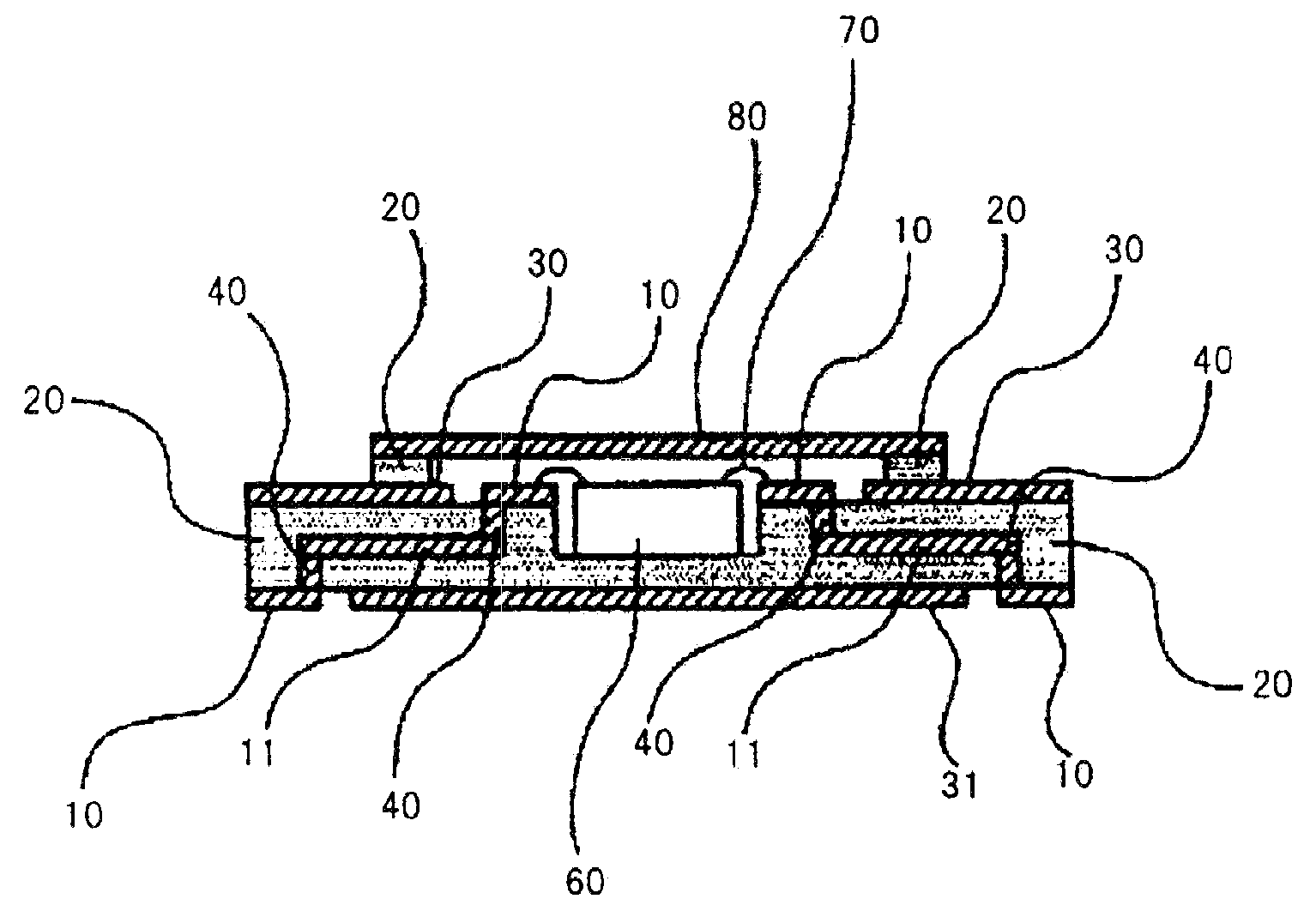
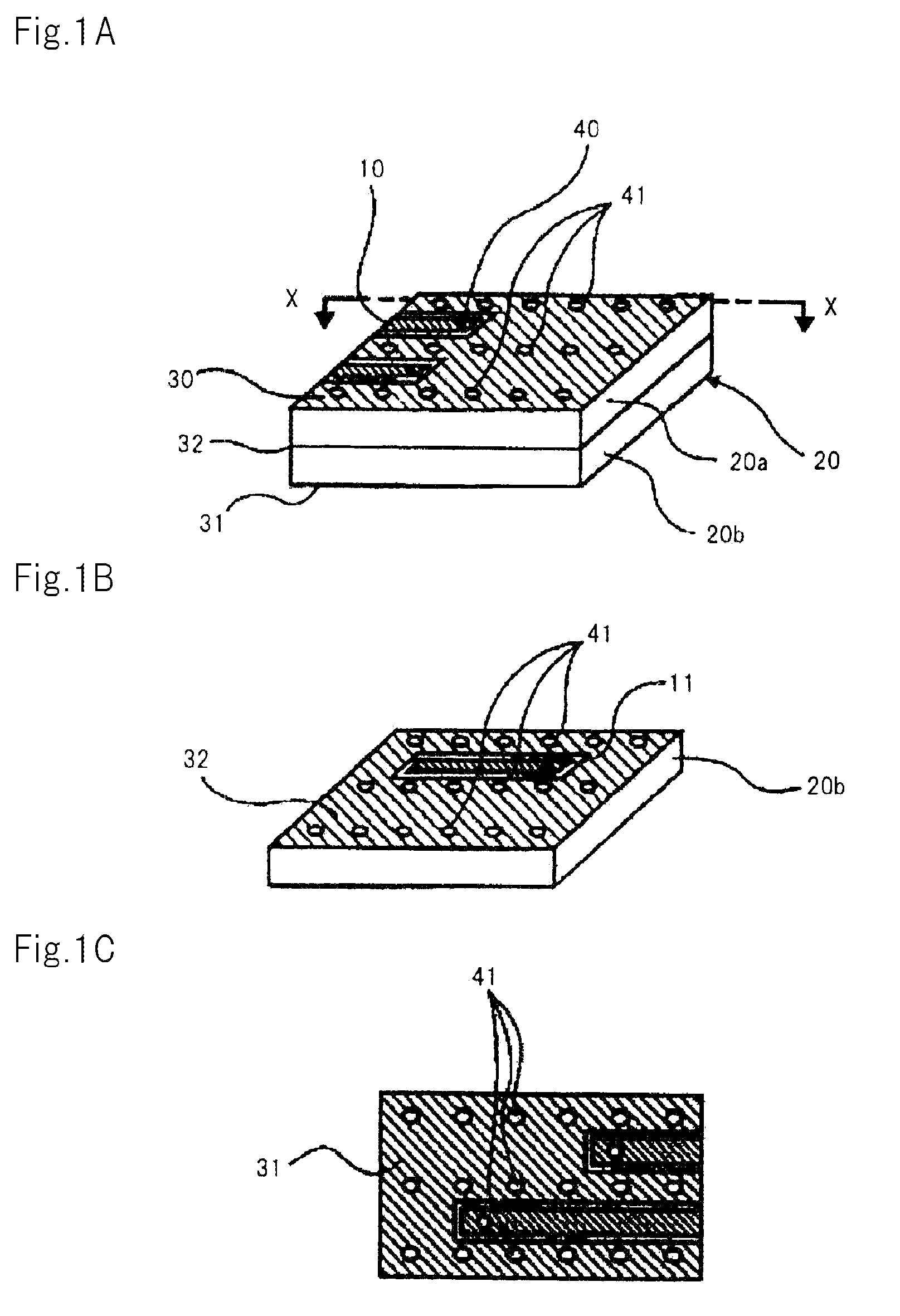
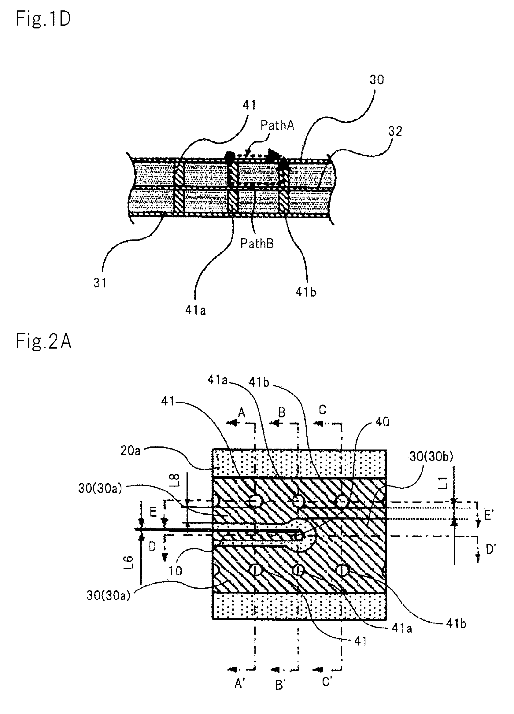
[0050]FIGS. 2A-2H show the construction of the high-frequency wiring board according to the first embodiment of the present invention. To state in greater detail, FIG. 2A is a plan view showing the first wiring layer of the high-frequency wiring board of the present embodiment; FIG. 2B is a plan view of the second wiring layer, and FIG. 2C is a plan view of the third wiring layer. FIG. 2D is a sectional view of the board taken along line A-A′ of FIG. 2A, FIG. 2E is a sectional view of the board taken along line B-B′ of FIG. 2A, FIG. 2F is a sectional view of the board taken along line C-C′ of FIG. 2A, FIG. 2G is a sectional view of the board taken along line D-D′ of FIG. 2A, and FIG. 2H is a sectional view of the board taken along line E-E′ of FIG. 2A. In each figure, the same reference numbers are used for functional parts that are the same as constituent elements shown in FIGS. 1A-1D.

[0051]The high-frequency wiring board of the present embodiment is composed of dielectric substrat...

second embodiment

[0095]FIGS. 7A-7H show a configuration of the high-frequency wiring board according to the second embodiment of the present invention. To state in greater detail, FIG. 7A is a plan view showing the first wiring layer of the high-frequency wiring board of the present embodiment, FIG. 7B is a plan view of the second wiring layer, and FIG. 7C is a plan view of the third wiring layer. FIG. 7D is a sectional view of the board taken along line A-A′ of FIG. 7A, FIG. 7E is a sectional view of the board taken along line B-B′ of FIG. 7A, FIG. 7F is a sectional view of the board taken along line C-C′ of FIG. 7A, FIG. 7G is a sectional view of the board taken along line D-D′ of FIG. 7A, and FIG. 7H is a sectional view of the board taken along line E-E′ of FIG. 7A. In each of the figures, the same reference numbers are used for functional parts that are the same as constituent elements shown in FIGS. 1A-1D.

[0096]The high-frequency wiring board of the present embodiment is made up of dielectric s...


PUM


Abstract

The high-frequency wiring board of the present invention is a wiring board that includes first coplanar lines and second coplanar lines formed on a different layer than the first coplanar lines; the first coplanar lines and second coplanar lines being connected at the line ends of each. The first coplanar lines are provided with a first signal line (10) and a first planar ground pattern (30a) formed on the same wiring layer as the first signal line (10). The second coplanar lines are provided with second signal line (11) formed on a wiring layer that differs from that of the first signal line (10), a second planar ground pattern 32 formed on the same wiring layer as the second signal line, and a first ground pattern (30b) formed on the same wiring layer as the first coplanar lines. The end of the first planar ground pattern (30a) and the end of the first ground pattern (30b) are connected and thus unified. In this high-frequency wiring board, the second planar ground pattern (32) is separated from the connection portion at the end of the first planar ground pattern (30a) in the direction in which the second coplanar lines extend from the vicinity of the connection portion of the first signal line and the second signal line.

Description

TECHNICAL FIELD[0001]The present invention relates to a high-frequency wiring board on which high-frequency transmission lines are formed, and more particularly to the interconnection of high-frequency transmission lines formed on different layers of a wiring board.BACKGROUND ART[0002]In high-frequency transmission lines used in, for example, packages for high-frequency semiconductor elements and wiring boards for mounting circuit elements, obverse-surface signal lines formed on the obverse surface of a dielectric substrate and intermediate-layer signal lines formed in the interior of the dielectric substrate are frequently interconnected by the relations of mounting positions of electronic components.[0003]Microstrip lines or coplanar lines are representative of obverse-surface signal lines that are formed on the obverse surface of a dielectric substrate, and strip lines and coplanar lines are representatively used as intermediate-layer signal lines that are formed within a dielect...

Claims


Application Information

Patent Timeline
Patent Type & Authority Applications(United States)
IPC IPC(8): H05K7/00H01P5/12
CPCH01P1/047H01L2224/48091H01L2224/48227H01L2924/15153H01L2924/15192H01L2924/15313H01L2924/16195
Inventor OHHIRA, RISATO
Owner NEC CORP
Why Eureka
Try Eureka