Eureka AIR delivers breakthrough ideas for toughest innovation challenges, trusted by R&D personnel around the world.

Leadframe for optical semiconductor device, method for manufacturing leadframe for optical semiconductor device, and optical semiconductor device

A technology for optical semiconductor devices and lead frames, which is applied to semiconductor devices, semiconductor/solid-state device components, optics, etc., and can solve problems such as reflectivity decline and reflectivity degradation.

Inactive Publication Date: 2012-12-26
FURUKAWA ELECTRIC CO LTD
View PDF7 Cites 10 Cited by
  • Summary
  • Abstract
  • Description
  • Claims
  • Application Information

AI Technical Summary

Problems solved by technology

[0009] In order to suppress the deterioration of the reflectivity of the lead frame material due to changes over time, methods such as alloying a metal with high reflectivity with a metal with excellent atmospheric resistance are sometimes used, but the decrease in reflectivity cannot be avoided.
Especially in metals such as silver and aluminum, which originally have high reflectance, the decrease in reflectance due to alloying is remarkable

Method used

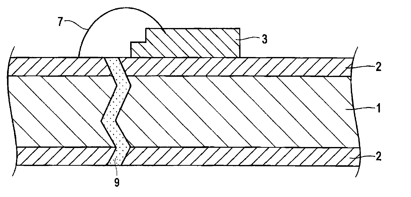
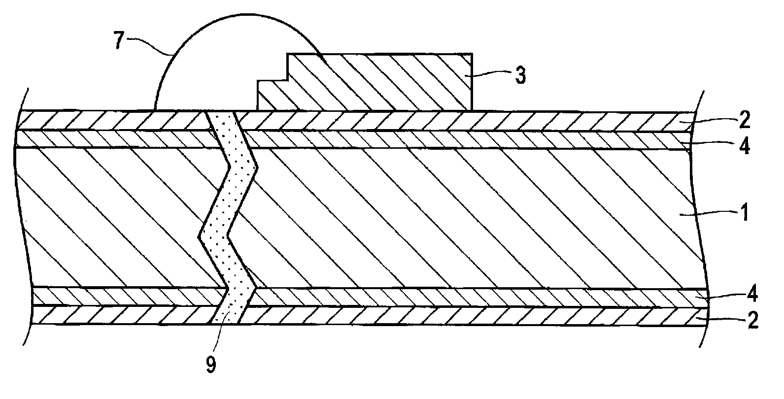
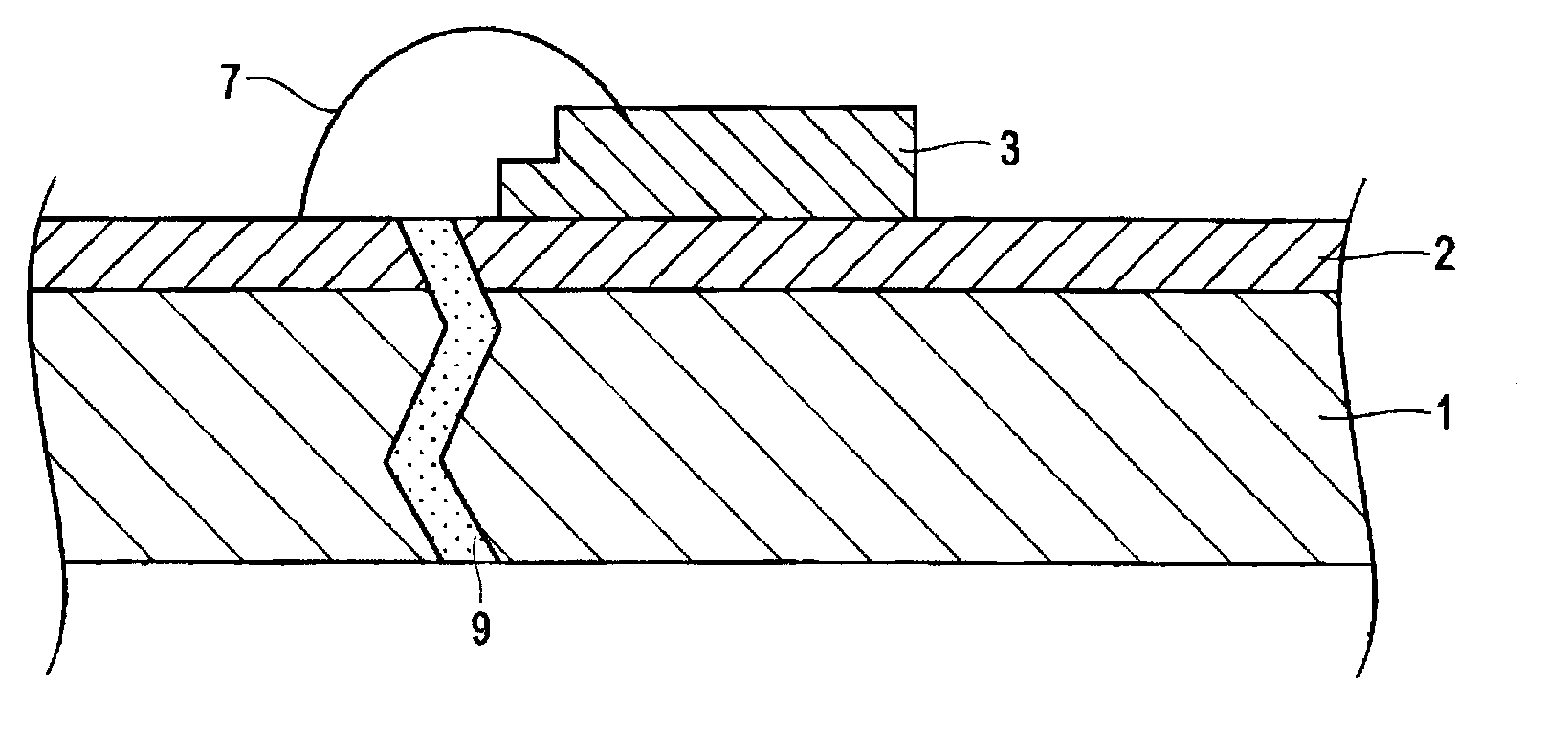

Image

  • Leadframe for optical semiconductor device, method for manufacturing leadframe for optical semiconductor device, and optical semiconductor device
  • Leadframe for optical semiconductor device, method for manufacturing leadframe for optical semiconductor device, and optical semiconductor device
  • Leadframe for optical semiconductor device, method for manufacturing leadframe for optical semiconductor device, and optical semiconductor device

Examples


Embodiment 1

[0179] As Example 1, after the pretreatment shown below was performed on the substrate with a width of 100 mm shown in Table 1, the plating treatment shown below was performed. In order to make the overall plate thickness including the coating thickness after rolling 0.2 mm, the plate thickness at the time of the initial formation of the reflective layer (during plating) was changed in consideration of the processing rate during the rolling process after the reflective layer was formed, and the thickness was changed by plating. Initially a reflective layer is formed. After that, using a 6-stage rolling mill (manufactured by Hitachi, Ltd.), using a roll with a surface roughness Ra of about 0.03 μm of the rolled workpiece roll, rolling was performed according to the area reduction ratio shown in Table 1 to a thickness of 0.2 mm, Thus, samples (rolled finished products) of Invention Examples 1 to 38 and Reference Examples 1 to 3 having the structures shown in Table 1 were obtaine...

Embodiment 2

[0249] As Example 2, the substrate shown in Table 3 with a width of 100 mm was pretreated in the same manner as in Example 1 above, and then subjected to the plating treatment shown in Table 3 in the same manner as in Example 1 above. Using a substrate with a plate thickness of 0.25 mm and 0.83 mm, Ag plating is performed on both sides of the substrate so that the Ag coating thickness after rolling is 3 μm, and the processing ratio during rolling after forming a reflective layer is 40%. Rolling is carried out to obtain strips with a plate thickness of 0.15 mm and 0.5 mm. After that, after performing blanking by pressing, plating was performed to form a plated film with good solder wettability only on the outer lead portion using a resist mask, and the resist was removed, and the results shown in Table 3 were obtained. Invention examples 39-50 and reference examples 6-9 of the structure.

[0250] In addition, in Conventional Examples 5 to 8, Ag plating was performed on strips ...

Embodiment 3

[0274] Example 3 is an example of an aspect characterized by the above-mentioned plating structure remaining rate.

[0275] As Example 3, the electroconductive substrate shown in Table 5 having a thickness of 0.25 mm and a width of 180 mm was subjected to the same pretreatment as above, and then subjected to plating treatment in the same manner as above. Thereafter, in order to plastically deform the Ag plating layer, the working rate was changed by rolling or pressing, and lead frames of Examples 101 to 121 of the present invention and Reference Example 101 were fabricated. Reference Example 102 simulated Comparative Example 1 of Patent Document 3, and Reference Example 103 simulated Example 2 of Patent Document 3, and prepared samples (heat-treated finished products) subjected to heat treatment at 240° C. for 4 hours after rolling. In addition, regarding the plated finished product of Conventional Example 101, after performing the same pretreatment as above on the conductive...


PUM

PropertyMeasurementUnit
surface roughnessaaaaaaaaaa
thicknessaaaaaaaaaa

Abstract

A lead frame for an optical semiconductor device, having a reflection layer at least on one side or each side of the outermost surface of a substrate, partially or entirely, in which the reflection layer has, on the outermost surface at least in a region where light emitted by an optical semiconductor element is reflected, a microstructure with at least the surface thereof having been mechanically deformed, which is converted from a plating microstructure formed of a metal or an alloy thereof; a method of producing the same, and an optical semiconductor device having the same.

Description

technical field [0001] The present invention relates to a lead frame for an optical semiconductor device, a manufacturing method thereof, and an optical semiconductor device. Background technique [0002] Lead frames for optical semiconductor devices are widely used as constituent members of various display / illumination light sources using light emitting elements such as LED (Light Emitting Diode) elements as light-emitting elements of optical semiconductor elements as light sources. Regarding this optical semiconductor device, for example, a lead frame is arranged on a substrate, and after a light emitting element is mounted on the lead frame, in order to prevent deterioration of the light emitting element or its surrounding parts caused by external factors such as heat, moisture, oxidation, etc., use The light-emitting element and its surroundings are sealed with resin or ceramics. [0003] In the case of an LED using a lead frame, a raw material such as a copper strip is...

Claims


Application Information

Patent Timeline
Patent Type & Authority Applications(China)
IPC IPC(8): H01L33/62
CPCH01L2924/0002H01L33/486H01L33/60H01L33/62C25D3/12C25D3/38C25D3/46C25D3/64C25D5/022C25D5/10C25D5/12C25D5/34C25D5/36C25D5/44C25D5/48C25D5/50C25D7/08C25D5/611C25D5/617C25D5/627H01L2224/48091H01L2924/00014H01L2924/00H01L23/49534H01L23/49579
Inventor 小林良聪松田晃铃木智菊池伸橘昭赖座间悟
Owner FURUKAWA ELECTRIC CO LTD
Why Eureka
Eureka Blog
Learn More