Integrated circuit having a filler standard cell

a filler standard and integrated circuit technology, applied in the field of forming integrated circuits, can solve the problems of short time to market cycles that do not allow such testing, increase the complexity of integrated circuits, and reduce the time to market for these complex integrated circuits

Inactive Publication Date: 2010-10-14
NXP USA INC
View PDF3 Cites 112 Cited by
  • Summary
  • Abstract
  • Description
  • Claims
  • Application Information

AI Technical Summary

Problems solved by technology

As customers demand more functionality on integrated circuits, the complexity of the integrated circuit increases.
In addition, the time to market for these complex integrated circuits is decreasing.
However, shorter time to market cycles do not allow for such testing.
Instead, semiconductor manufacturers place test devices in the streets, which are the spaces between die, on the production wafers themselves, greatly limiting the number of structures available for characterization.

Method used


Image

  • Integrated circuit having a filler standard cell
  • Integrated circuit having a filler standard cell
  • Integrated circuit having a filler standard cell

Examples


Embodiment Construction

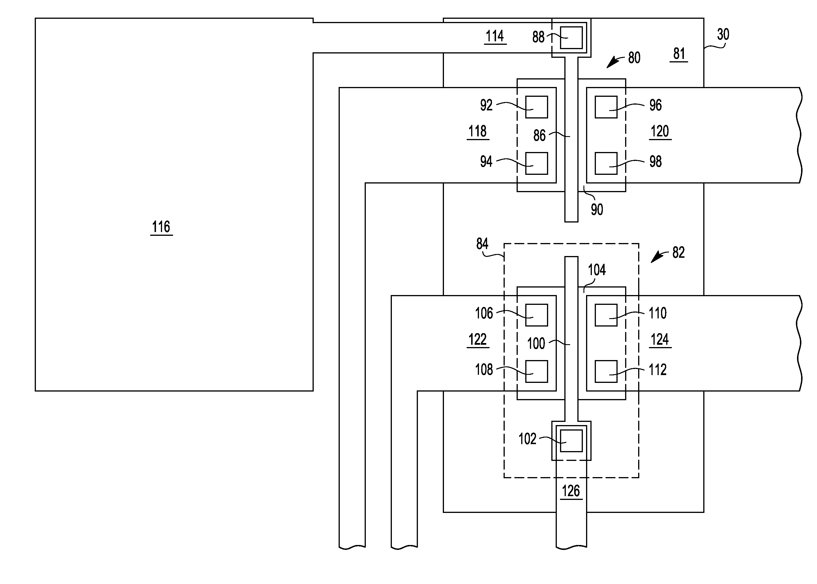
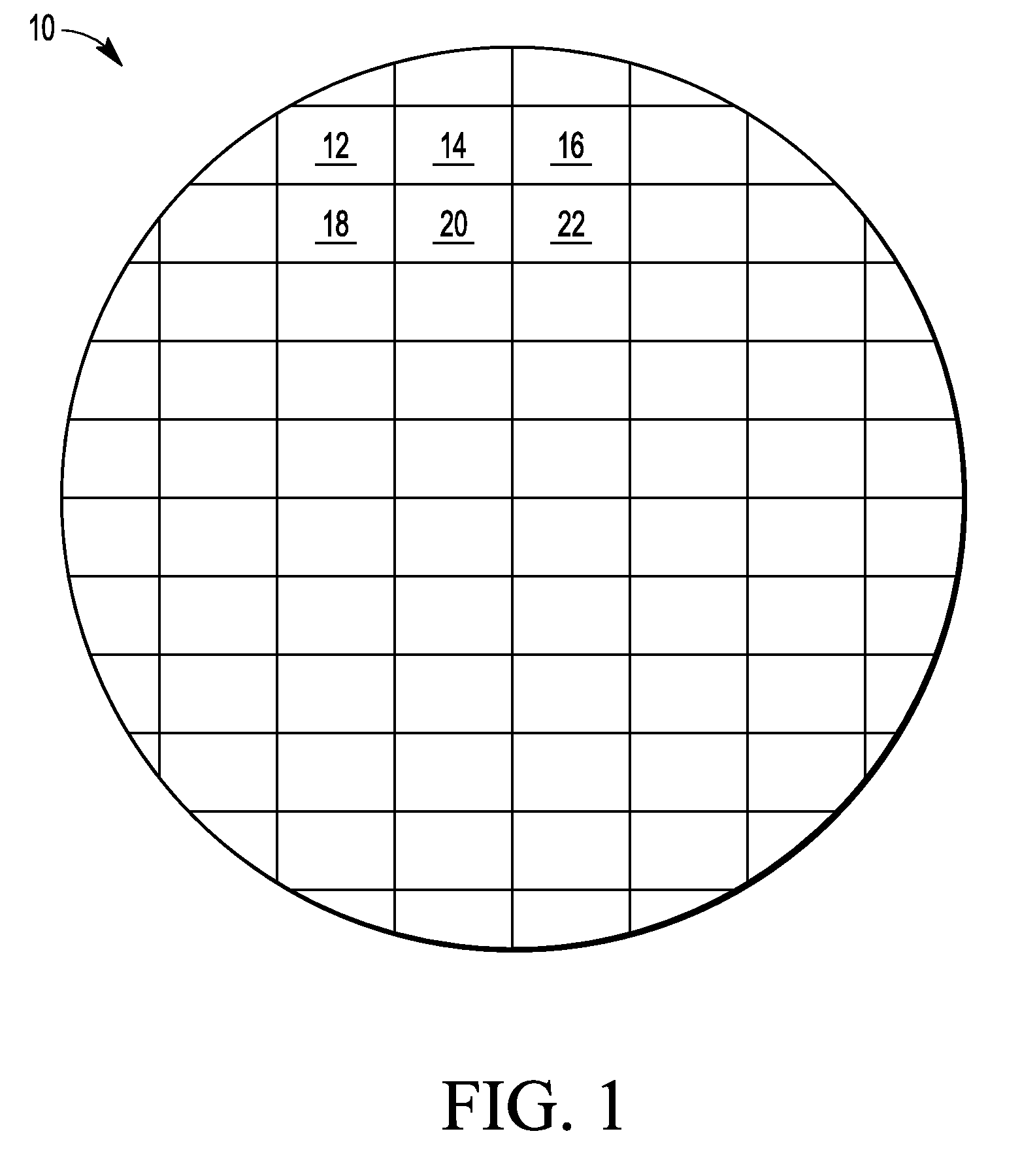
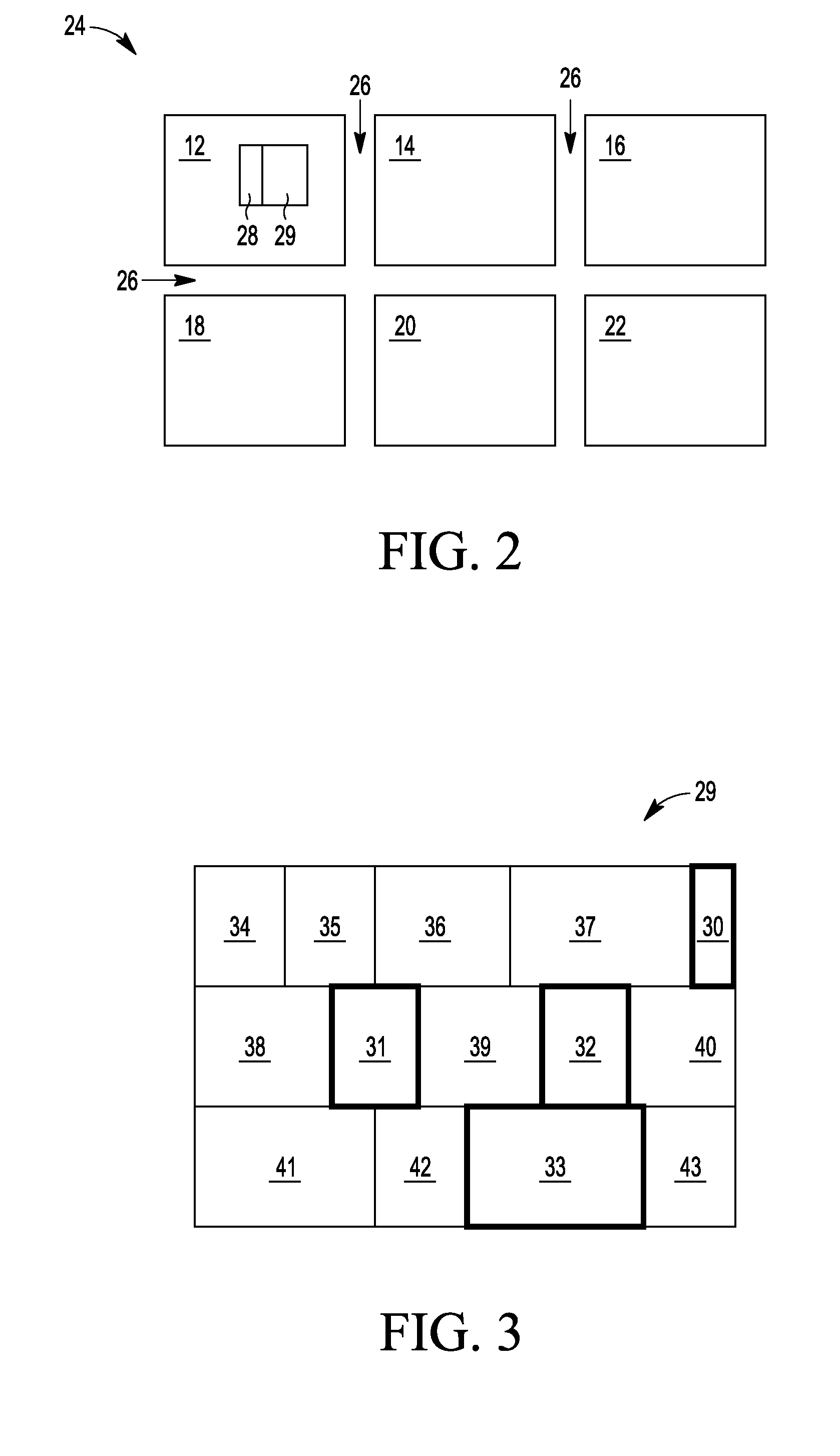
[0011]Test devices can be formed in the streets on production wafers because they are not needed for the functioning of the integrated circuit and hence their destruction or removal during die singulation does not impact the integrated circuit. (An integrated circuit may also be referred to as a semiconductor device.) In other words, test devices can be formed in the area between die on wafers. However, the area of the street limits the number of test devices that can be formed in the streets. Test devices can be formed, instead or in addition to those in the streets, in standard blocks (e.g., filler standard cells) within die. In one embodiment, filler standard cells can be modified to include test devices. Filler standard cells are blocks that are added to the wafer to fill empty space so that there is a consistent density across the wafer. Among other things, this consistent density may be useful for chemical mechanical polishing uniformity. In addition, filler standard cells may...


PUM


Abstract

An integrated circuit includes a functional block having a plurality of standard cells. The plurality of standard cells includes a plurality of functional standard cells and a filler standard cell. Each functional standard cell of the plurality of functional standard cells has a rectangular boundary. The filler standard cell has a rectangular boundary adjacent to at least one of the functional standard cells. The filler standard cell is selectable between a first state and a second state. The filler standard cell is non-functional in the first state. The filler standard cell has functional test structures coupled to a first metal layer in the second state. This allows for test structures helpful in analyzing functionality of circuit features such as transistors without requiring additional space on the integrated circuit.

Description

BACKGROUND[0001]1. Field[0002]This disclosure relates generally to forming an integrated circuit and more specifically, to forming filler standard cells in an integrated circuit.[0003]2. Related Art[0004]As customers demand more functionality on integrated circuits, the complexity of the integrated circuit increases. In addition, the time to market for these complex integrated circuits is decreasing. In the past, semiconductor manufacturers would manufacture test wafers having test devices to determine and fix problems, such as yield, before production wafers were manufactured. However, shorter time to market cycles do not allow for such testing. Instead, semiconductor manufacturers place test devices in the streets, which are the spaces between die, on the production wafers themselves, greatly limiting the number of structures available for characterization.BRIEF DESCRIPTION OF THE DRAWINGS[0005]The present invention is illustrated by way of example and is not limited by the accomp...

Claims


Application Information

Patent Timeline
Patent Type & Authority Applications(United States)
IPC IPC(8): H01L27/00G06F17/50
CPCH01L22/34
Inventor SOKEL, RALPH J.WORKMAN, GLENN O.
Owner NXP USA INC
Why Eureka
Try Eureka