Methods and apparatus for epitaxial growth of semiconductor materials

a technology of epitaxial growth and semiconductor materials, applied in the field of semiconductor materials, can solve the problems of wasting precursors and contamination of reactors

Inactive Publication Date: 2010-10-21
ZHIYIN GAN
View PDF15 Cites 90 Cited by
  • Summary
  • Abstract
  • Description
  • Claims
  • Application Information

AI Technical Summary

Problems solved by technology

Many conventional reactors have the problem of pre-reaction and ceiling-coating, which can result in wasting of the precursors and contamination of the reactor.

Method used


Image

  • Methods and apparatus for epitaxial growth of semiconductor materials
  • Methods and apparatus for epitaxial growth of semiconductor materials
  • Methods and apparatus for epitaxial growth of semiconductor materials

Examples


Embodiment Construction

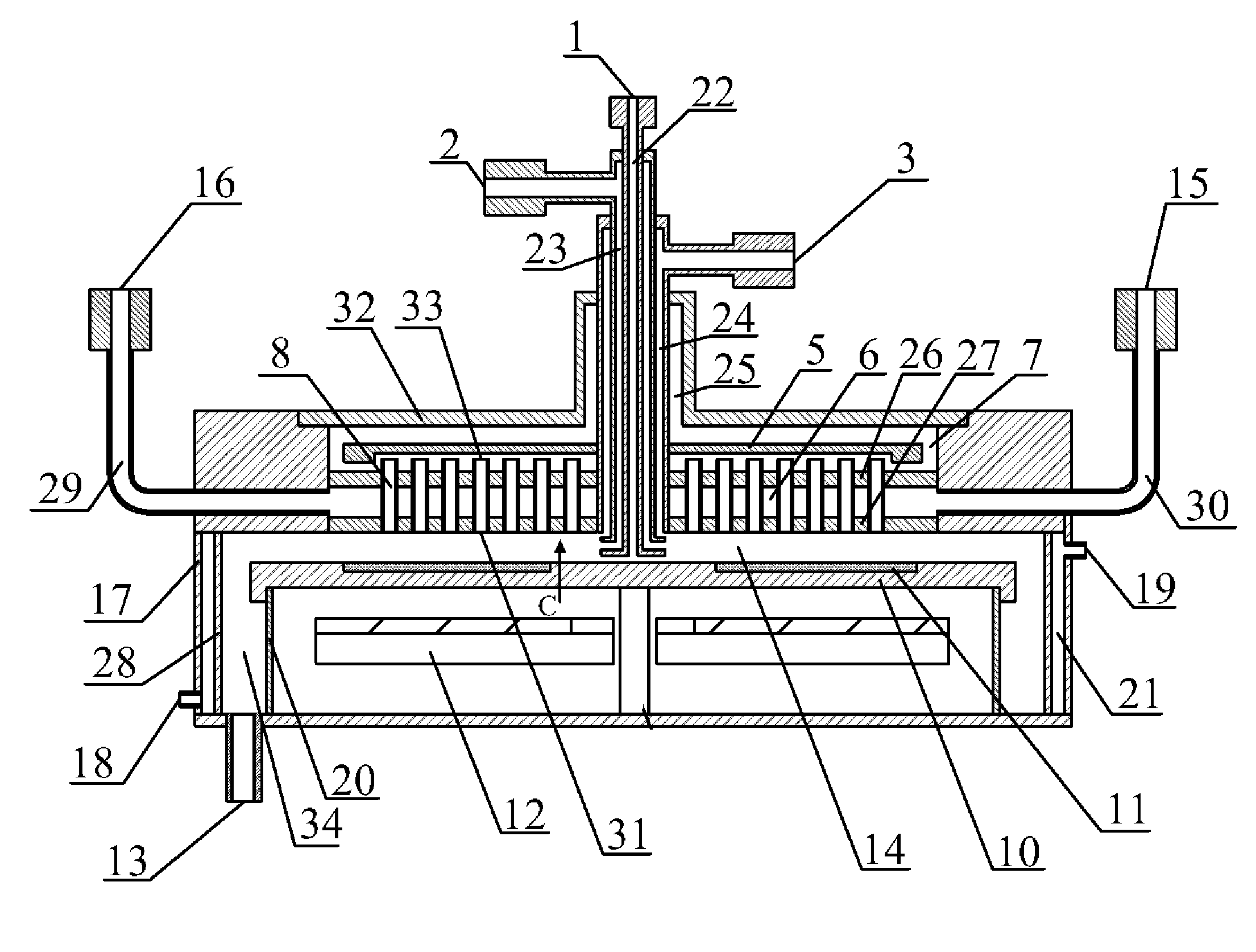
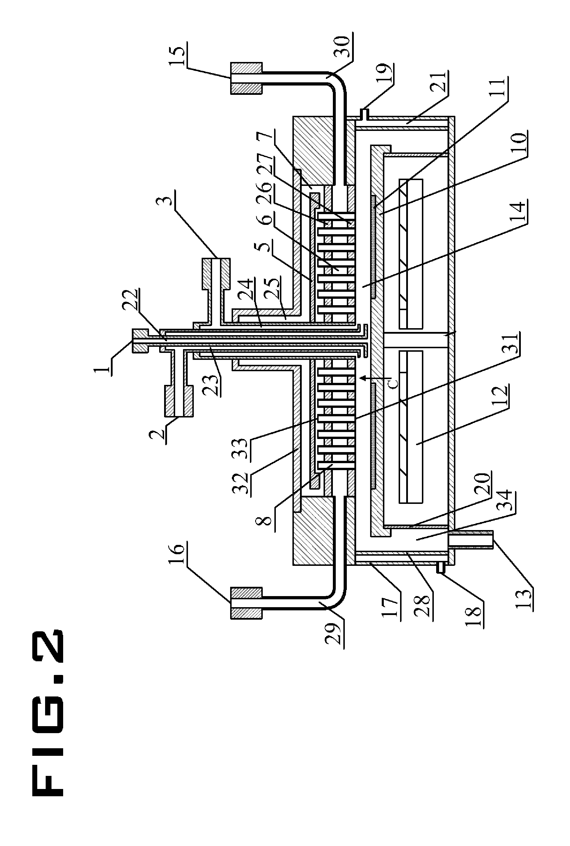
[0016]The present invention overcomes and / or minimizes the problems discussed above by separately introducing the gaseous precursors into the reaction chamber and combining the advantages of radial flow of vertical injection reactors and traditional showerhead structure, which emits the reactants to the heated substrate on the susceptor through thousands of vertical nozzles.

[0017]According to a first aspect of the present invention, an apparatus for growing epitaxial layers on one or more wafers by chemical vapor deposition is provided, which reactor comprises:

[0018](1) a reaction chamber for accommodating a heated substrate upon which said material is to be deposited by reaction of said precursors,

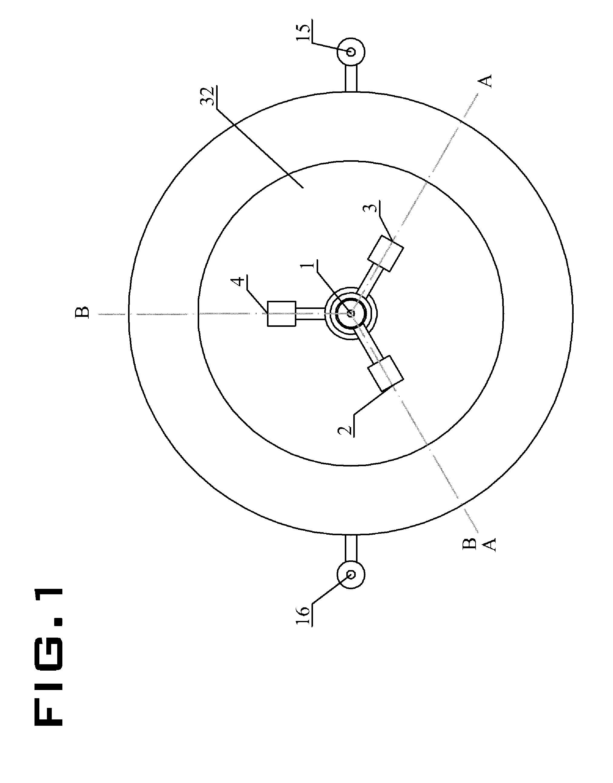
[0019](2) three concentric central conduits connecting the reaction chamber for the first, second and third precursors,

[0020](3) a first chamber for the fourth precursor has a baffle plate inside,

[0021](4) hundreds of conduits connecting the first chamber to the reaction chamber to provid...


PUM

PropertyMeasurementUnit
semiconductoraaaaaaaaaa
crystal latticeaaaaaaaaaa
crystal lattice structuresaaaaaaaaaa

Abstract

Epitaxial growth of semiconductor materials is carried out by introducing two or more reaction gases along with their carrier gas into a reaction chamber via one or more concentric pipe inlets and a plurality of separately distributed injection ports with a gas distribution system. The reaction gas can be injected into the reaction chamber either continuously or in pulse mode, wherein reaction gases are mixed together or injected alternately into the reaction chamber. The semiconductor materials are deposited on the substrates which are located on the rotating heated susceptor within the reaction chamber.

Description

FIELD OF THE INVENTION[0001]The invention relates generally to semiconductors. More particularly, the invention relates to epitaxial growth of semiconductor materials.BACKGROUND OF THE INVENTION[0002]The present invention relates to epitaxial growth and more particularly, but not exclusively, is concerned with metal organic chemical vapor deposition (MOCVD) and atomic layer deposition (ALD).[0003]It is known that the CVD processes, if properly controlled, produce thin films having organized crystal lattice. Especially important are the thin films having the same crystal lattice structures as the underlying substrates. The layers by which such thin films grow are called the epitaxial layers. MOCVD is considered as an important technique to achieve epitaxial growth of semiconductor and high temperature compounds such as GaAs, InP, GaN, AlGaAs, and InGaAsP. The epitaxial layers are typically grown by causing appropriate reactant chemicals in gaseous form to flow over the wafers in cont...

Claims


Application Information

Patent Timeline
Patent Type & Authority Applications(United States)
IPC IPC(8): C30B25/10C23C16/22C30B25/02
CPCC23C16/45508C23C16/45544C23C16/45572C23C16/45574C30B25/14
Inventor ZHIYIN, GAN
Owner ZHIYIN GAN
Why Eureka
Try Eureka