Input/output circuit and integrated circuit apparatus including the same

a technology of input/output circuit and integrated circuit, which is applied in the direction of logic circuit coupling/interface arrangement, pulse technique, instruments, etc., can solve the problems of increasing increasing the cost of input/output circuit, and increasing the cost of input/output transistors. , to achieve the effect of reducing the reliability of gate oxide and preventing or reducing leakage curren

Active Publication Date: 2010-10-28
SAMSUNG ELECTRONICS CO LTD
View PDF6 Cites 17 Cited by
  • Summary
  • Abstract
  • Description
  • Claims
  • Application Information

AI Technical Summary

Benefits of technology

[0012]Exemplary embodiments of the present inventive concept also provide an I/O circuit for preventing or reducing leakage current under low voltage operating conditions.
[0013]Exemplary embodiments of the present inventive concept also provide an I/O circuit for reducin

Problems solved by technology

When a conventional non-mixed interfacing method is used in a mixed-voltage system, generation of unwanted leakage current, decrease in the reliability of a gate oxide, and hot-carrier injection may occur.
However, these conventional methods need additional pads or transistors connected in complicated ways.
Moreover, some of the conventional methods increase I/O pad loading and pull-up gate loading, which may decrease I/O interface speed.
Th

Method used


Image

  • Input/output circuit and integrated circuit apparatus including the same
  • Input/output circuit and integrated circuit apparatus including the same
  • Input/output circuit and integrated circuit apparatus including the same

Examples


Embodiment Construction

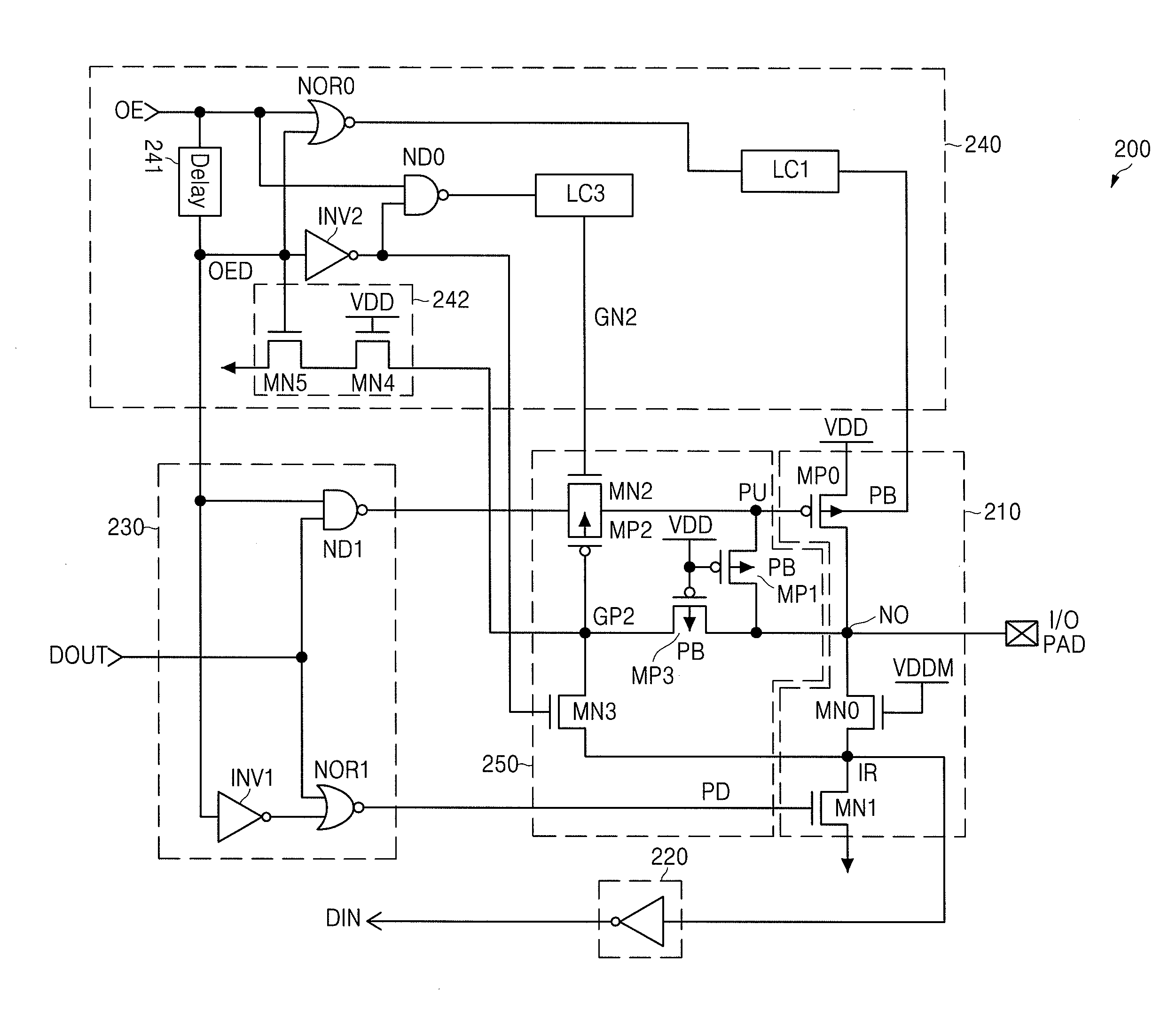
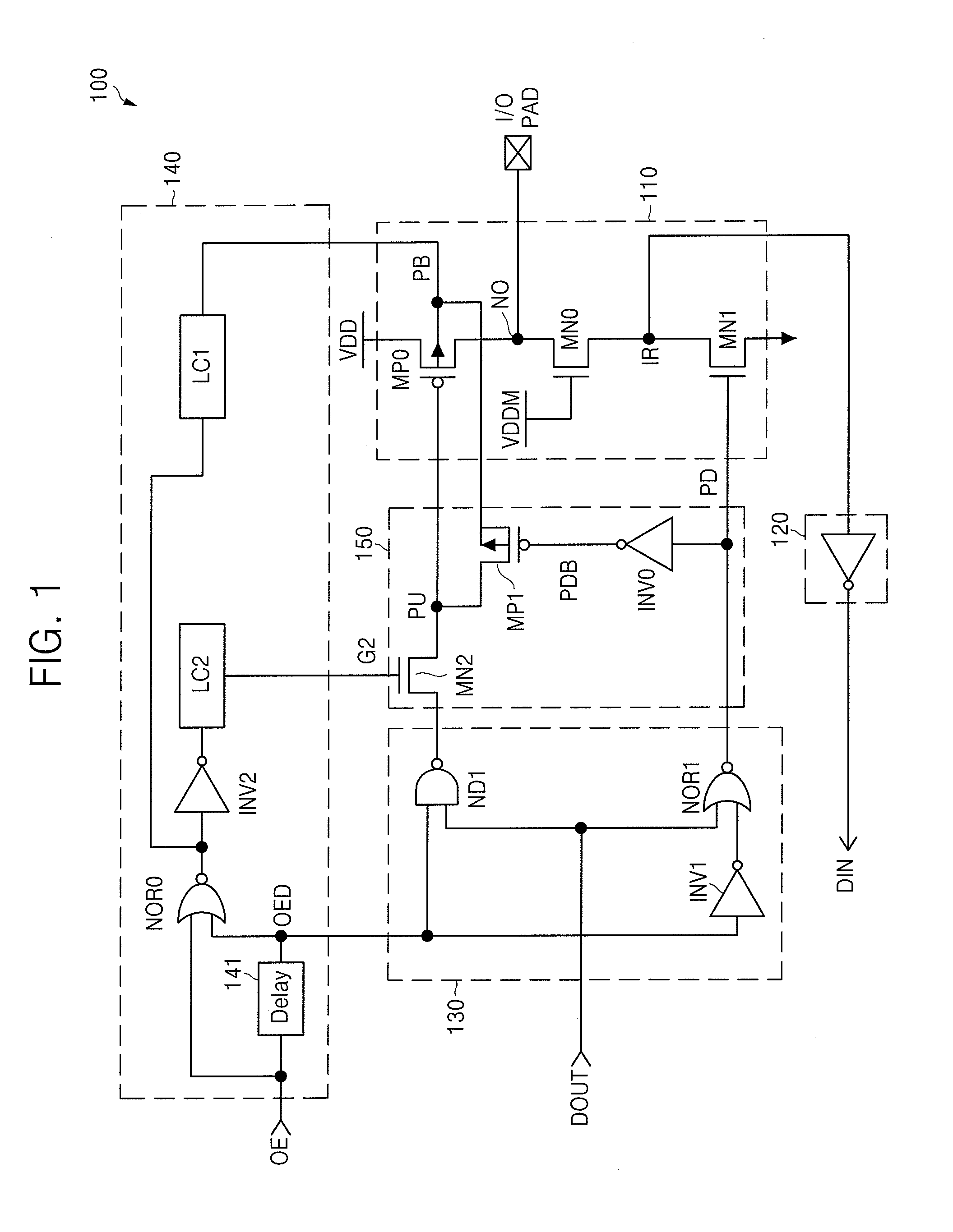
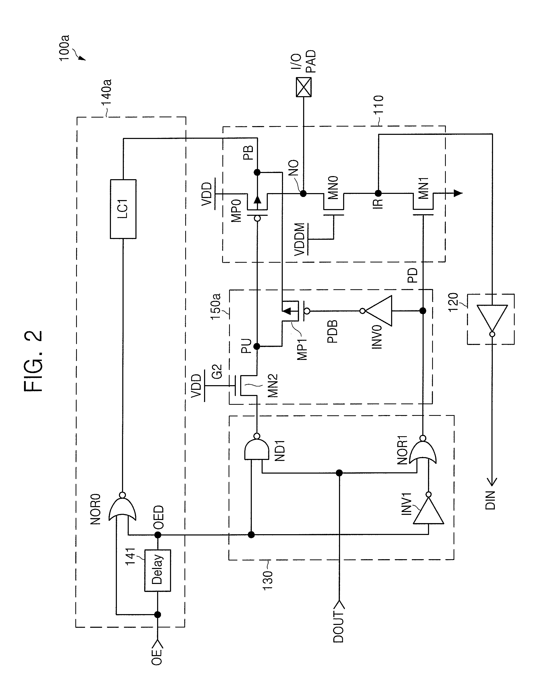
[0062]The present inventive concept will be described more fully hereinafter with reference to the accompanying drawings, in which exemplary embodiments are shown. The present inventive concept may, however, be embodied in many different forms and should not be construed as limited to the exemplary embodiments set forth herein. In the drawings, like numbers refer to like elements throughout.

[0063]It will be understood that when an element is referred to as being “connected” or “coupled” to another element, it can be directly connected or coupled to the other element or intervening elements may be present.

[0064]It will be also understood that, although the terms first, second, etc. may be used herein to describe various elements, these elements should not be limited by these terms. These terms are only used to distinguish one element from another. For example, a first signal could be termed a second signal, and, similarly, a second signal could be termed a first signal without depart...


PUM


Abstract

An input/output circuit includes an I/O node connected to a pull up and pull down circuit having a pull up and pull down transistors. Data is sent and received at through the I/O node. A level shifter provides voltages including a supply voltage and a high voltage higher than the supply voltage. A signal control circuit controls the voltage level applied to the pull up and pull down circuit. During a data input mode, data is received at the I/O node and the pull up transistor is biased at the high voltage to cut off the pull up transistor. During a data output mode, data is output at the I/O node and the pull down transistor pulls down the I/O node to ground when the output data is low, and the pull up transistor is activated when the output data is high.

Description

CROSS-REFERENCE TO RELATED APPLICATION[0001]This application claims under 35 U.S.C. §119 priority to and the benefit of Korean Patent Application No. 10-2009-0034870 filed on Apr. 22, 2009, in the Korean Intellectual Property Office, the entire content of which is incorporated by reference herein.BACKGROUND[0002]1. Technical Field[0003]The present disclosure relates to an integrated circuit (IC) apparatus, and more particularly, to a mixed-voltage input / output (I / O) circuit for interfacing apparatuses having different operating voltages and an IC apparatus including the same.[0004]2. Discussion of Related Art[0005]In complementary metal-oxide semiconductor (CMOS) technology, a supply voltage is scaled down to reduce power consumption and the dimensions of a transistor are also scaled down to improve circuit performance and area efficiency. Some semiconductor chips in a microelectronic system are implemented using different CMOS techniques and cannot use the same voltage, and therefo...

Claims


Application Information

Patent Timeline
IPC IPC(8): H03K19/0175G11C7/00
CPCG11C7/1051G11C7/1057G11C7/1078H04L25/0278G11C7/22H03K19/017509G11C7/1084G11C5/14G11C7/10
Inventor KIM, JOUNG YEALJUN, YOUNG HYUNKONG, BAI SUN
Owner SAMSUNG ELECTRONICS CO LTD
Why Eureka
Try Eureka