Multilayer ceramic electronic component

a technology of electronic components and ceramics, applied in the direction of fixed capacitors, fixed capacitor details, capacitors, etc., can solve the problems of difficult to ensure the quality of multilayer ceramic capacitors, limit the effective area of internal electrodes, and easy occurrence of short circuits between internal electrodes

Active Publication Date: 2010-10-28
MURATA MFG CO LTD
View PDF31 Cites 27 Cited by
  • Summary
  • Abstract
  • Description
  • Claims
  • Application Information

AI Technical Summary

Benefits of technology

[0013]Accordingly, preferred embodiments of the present invention provide a multilayer ceramic electronic component that can solve the problems described above.
[0019]In the exposed area defined by the exposed portions of the internal conductors, a relatively large amount of constituent metal of the internal conductors is scattered in the end section of the exposed area during a polishing process. According to preferred embodiments of the present invention, the area ratio of the exposed portions in the end section of the exposed area is preferably smaller than that of the exposed portions in the center section of the exposed area. With this configuration, the amount of metal scattered in the end section of the exposed area can be relatively reduced. Ideally, with this configuration, the amount of scattered metal can be made substantially uniform in the stacking direction of the ceramic body.
[0020]Therefore, even when plating films grow around pieces of metal scattered in the polishing process, the external terminal electrodes formed by the plating films can be prevented from being partially widened near outer layers of the ceramic body. Thus, even when the external terminal electrodes are formed side by side on one side surface of the ceramic body, it is possible to prevent easy occurrence of solder bridging, which creates an undesired connection between adjacent external terminal electrodes during mounting.

Problems solved by technology

Although there is currently a demand for thinner dielectric ceramic layers, use of thinner dielectric ceramic layers leads to easier occurrence of short circuits between internal electrodes.
This makes it difficult to ensure quality of the multilayer ceramic capacitors.
This means that there is a limit to increasing the effective area of the internal electrodes.
However, it is difficult to increase the area of the dielectric ceramic layers within specified dimensions.
Additionally, the thickness of external terminal electrodes is an obstacle to increasing the area of the dielectric ceramic layers.
Forming the external terminal electrodes 3 having the shape of FIG. 18 may lead to a problem called solder bridging, which creates an undesired connection between adjacent external terminal electrodes 3 during mounting.

Method used


Image

  • Multilayer ceramic electronic component
  • Multilayer ceramic electronic component
  • Multilayer ceramic electronic component

Examples


Embodiment Construction

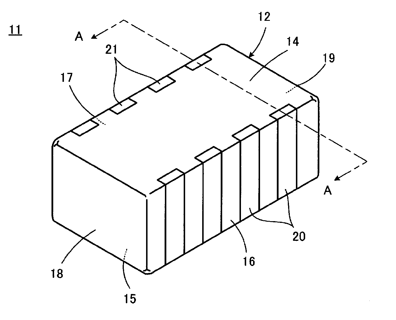
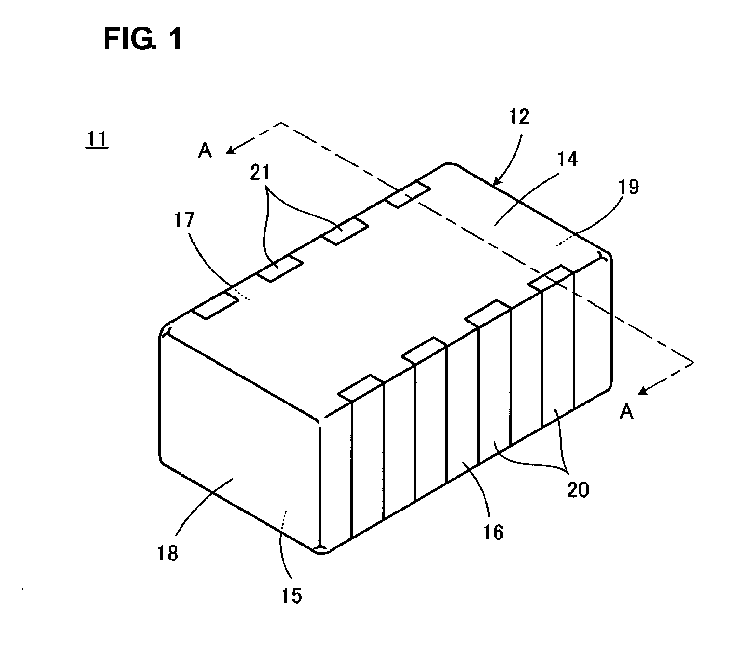
[0040]A multilayer ceramic electronic component 11 according to a first preferred embodiment of the present invention will be described with reference to FIG. 1 to FIG. 7.

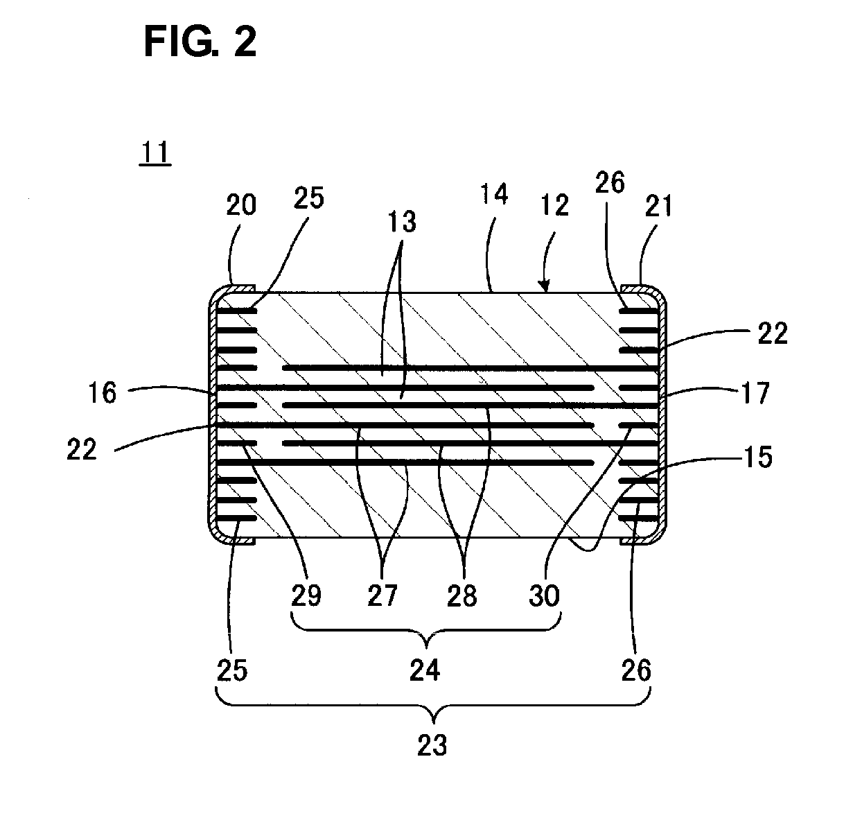
[0041]As illustrated in FIG. 1 to FIG. 3F, a ceramic body 12 of the multilayer ceramic electronic component 11 includes a plurality of stacked ceramic layers 13. The ceramic body 12 has a first principal surface 14 and a second principal surface 15 opposite each other, and first to fourth side surfaces 16 to 19 that connect the first and second principal surfaces 14 and 15. The first side surface 16 and the second side surface 17 are opposite each other, and the third side surface 18 and the fourth side surface 19 are opposite each other.

[0042]As can be seen from FIG. 1 to FIG. 4 and FIG. 7, corners and ridges between adjacent ones of the principal surfaces 14 and 15 and side surfaces 16 to 19 of the ceramic body 2 are rounded.

[0043]As clearly illustrated in FIG. 1, the multilayer ceramic electronic component 11 is...


PUM

PropertyMeasurementUnit
thicknessaaaaaaaaaa
thicknessaaaaaaaaaa
thicknessaaaaaaaaaa

Abstract

In a multilayer ceramic electronic component, in an exposed area defined by exposed portions of a plurality of internal conductors, an area ratio of exposed portions in an end section of the exposed area is smaller than that of exposed portions in a center section of the exposed area.

Description

BACKGROUND OF THE INVENTION[0001]1. Field of the Invention[0002]The present invention relates to multilayer ceramic electronic components, and particularly to a multilayer ceramic electronic component in which external terminal electrodes are formed by direct plating such that the external terminal electrodes are electrically connected to a plurality of internal conductors.[0003]2. Description of the Related Art[0004]In recent years, the market for small portable electronic devices, such as mobile phones, notebook computers, digital cameras, and digital audio devices, has been expanded. These portable electronic devices have been reduced in size and improved in performance. Accordingly, multilayer ceramic electronic components included, in large numbers, in such portable electrical devices are demanded to be smaller in size and higher in performance. For example, multilayer ceramic capacitors are demanded to be smaller in size and larger in capacitance.[0005]An effective way to real...

Claims


Application Information

Patent Timeline
Patent Type & Authority Applications(United States)
IPC IPC(8): H01G4/30
CPCH01G4/012H01G4/30H01G4/232
Inventor SASABAYASHI, TAKEHISA
Owner MURATA MFG CO LTD
Why Eureka
Try Eureka