

Method for cleaning a ceramic member for use in a system for producing semiconductors, a cleaning agent and a combination of cleaning agents
a technology for ceramic parts and semiconductors, applied in the direction of thermoelectric devices, cleaning using liquids, inorganic non-surface active detergent compositions, etc., can solve the problems of off-specification products, low-level metal contamination, etc., and achieve the effect of reducing the amount of metal atoms transferred
- Summary
- Abstract
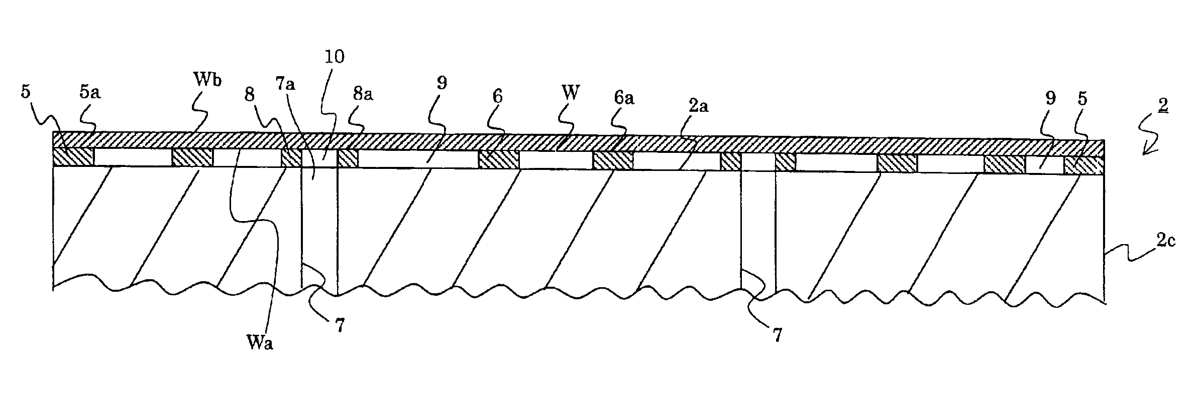
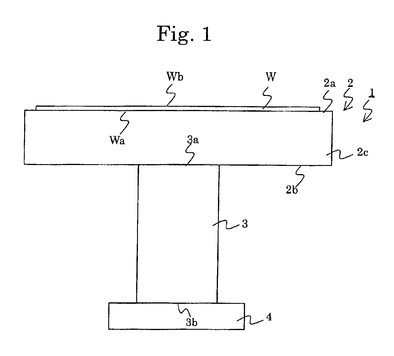
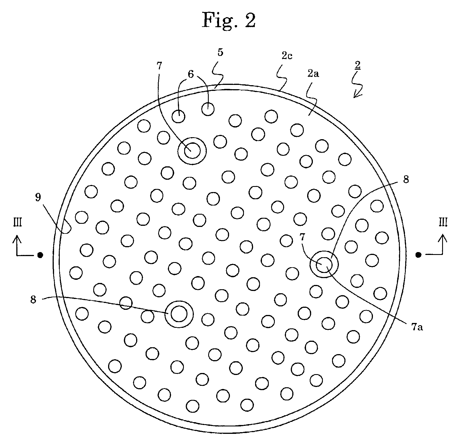
- Description
- Claims
- Application Information
AI Technical Summary
Benefits of technology
Problems solved by technology
Method used
Image

Examples
example 1
The ceramic member 2 was manufactured and then the semiconductor mounting surface was subjected to blasting as in comparative example 2. Then it was cleansed by aqueous solution of oxalic acid. The concentration of oxalic acid was 1N and the treatment was performed for 5 minutes. As a result, the count number of copper was 4.7×10¹⁰ atoms / cm2.
example 2
In the example 1, the concentration of oxalic acid was variously changed in the range of 0.01 to 1 N. As a result, the count number of copper was 4.7 to 6.6×10¹⁰ atoms / cm2.
example 3
In the example 1, the time period for the treatment with oxalic acid was variously changed in the range of 1 to 10 min. As a result, the count number of copper was 4.7 to 6.0×10¹⁰ atoms / cm2. From these results, it was proved that the concentration of oxalic acid and the treatment time period did not substantially affect the results.
PUM
| Property | Measurement | Unit |
|---|---|---|
| temperature | aaaaa | aaaaa |
| height | aaaaa | aaaaa |
| diameter | aaaaa | aaaaa |
Abstract
Description
Claims
Application Information