Fabrication process of a semiconductor device

a technology of semiconductor devices and fabrication processes, applied in the direction of semiconductor devices, electrical devices, transistors, etc., can solve the problems of reducing the gate length and other problems

Inactive Publication Date: 2007-07-19
FUJITSU SEMICON LTD
View PDF1 Cites 14 Cited by
  • Summary
  • Abstract
  • Description
  • Claims
  • Application Information

AI Technical Summary

Benefits of technology

[0014] According to this conventional technology of elevated silicide formation, the metal atoms on the surface part of the metallic film are consumed by the silicide formation reaction caused by the silane gas by supplying the silane gas to the surface of the metallic film at the time of the reaction between the metallic film and the silicon surface as noted before, and the amount of the metal atoms causing reaction with the silicon surface is reduced. With this, it becomes possible to reduce the depth of the silicide layer formation region invading into the silicon substrate.
[0036] According to the present invention, it becomes possible to form a nickel silicide layer having a composition represented by Ni2Si at the interface between the silicon surface and the metallic nickel film formed thereon while suppressing the occurrence of silicide formation reaction in the entire metallic silicide film and suppressing at the same time excessive invasion of Ni atoms into the silicon surface from the metallic silicide film, by conducting the silicide forming reaction in a silane gas ambient at a temperature of 220° C. or less. Thus, by converting such a nickel silicide layer to a nickel monosilicide layer of the composition of NiSi by conducting a thermal annealing process, it becomes possible to form a low-resistance nickel monosilicide layer stably with shallow depth.

Problems solved by technology

Today, there is already realized a semiconductor device having a gate length of 100 nm or less, while with such ultra-miniaturized semiconductor devices, there arise various problems in relation to decrease of the gate length.

Method used


Image

  • Fabrication process of a semiconductor device
  • Fabrication process of a semiconductor device
  • Fabrication process of a semiconductor device

Examples


first embodiment

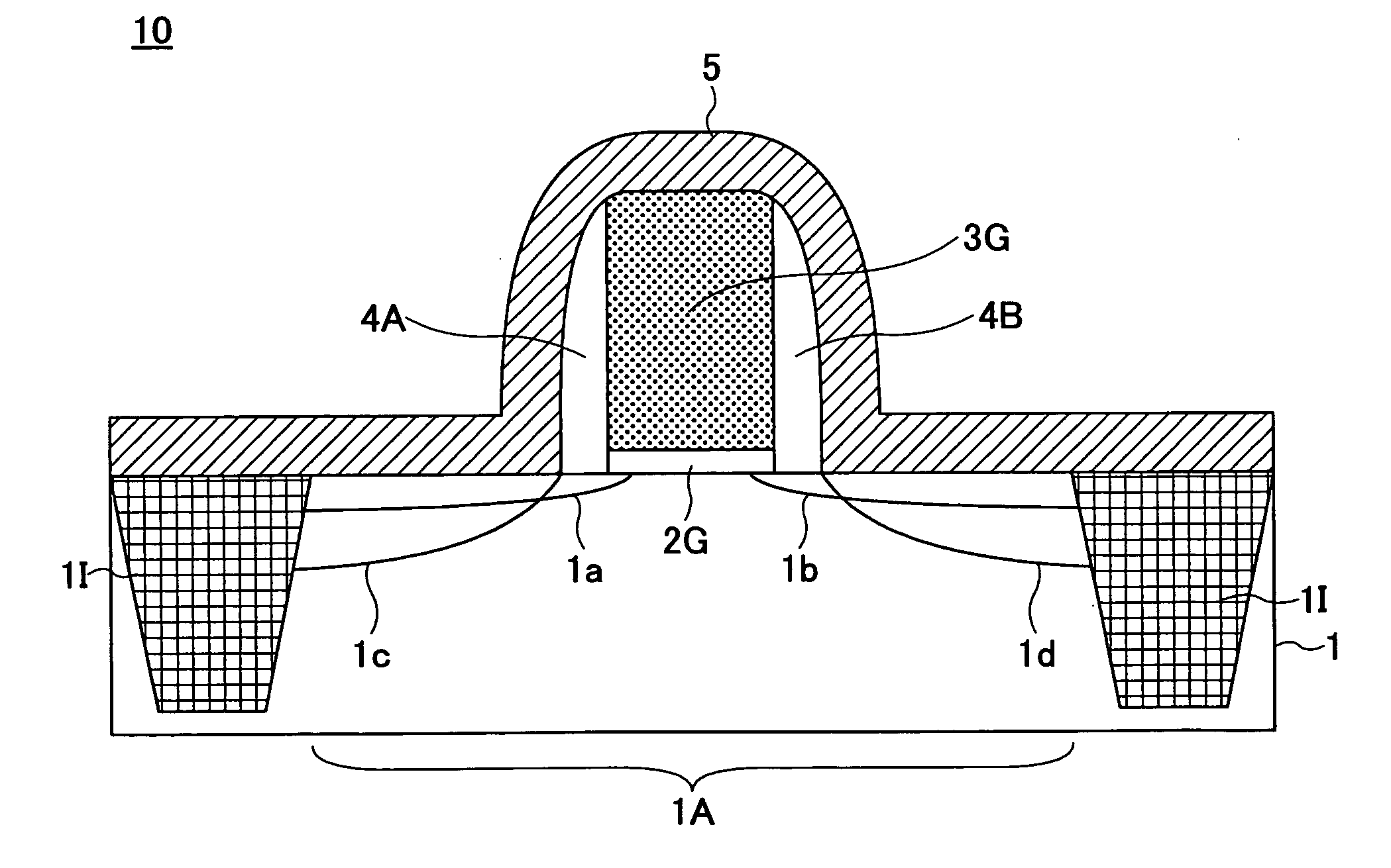
[0044]FIGS. 1A-1L are diagrams showing the outline of the fabrication process of a semiconductor device 10 according to a first embodiment of the present invention, while FIG. 2 shows the flowchart corresponding to the steps of FIGS. 1H-1L.

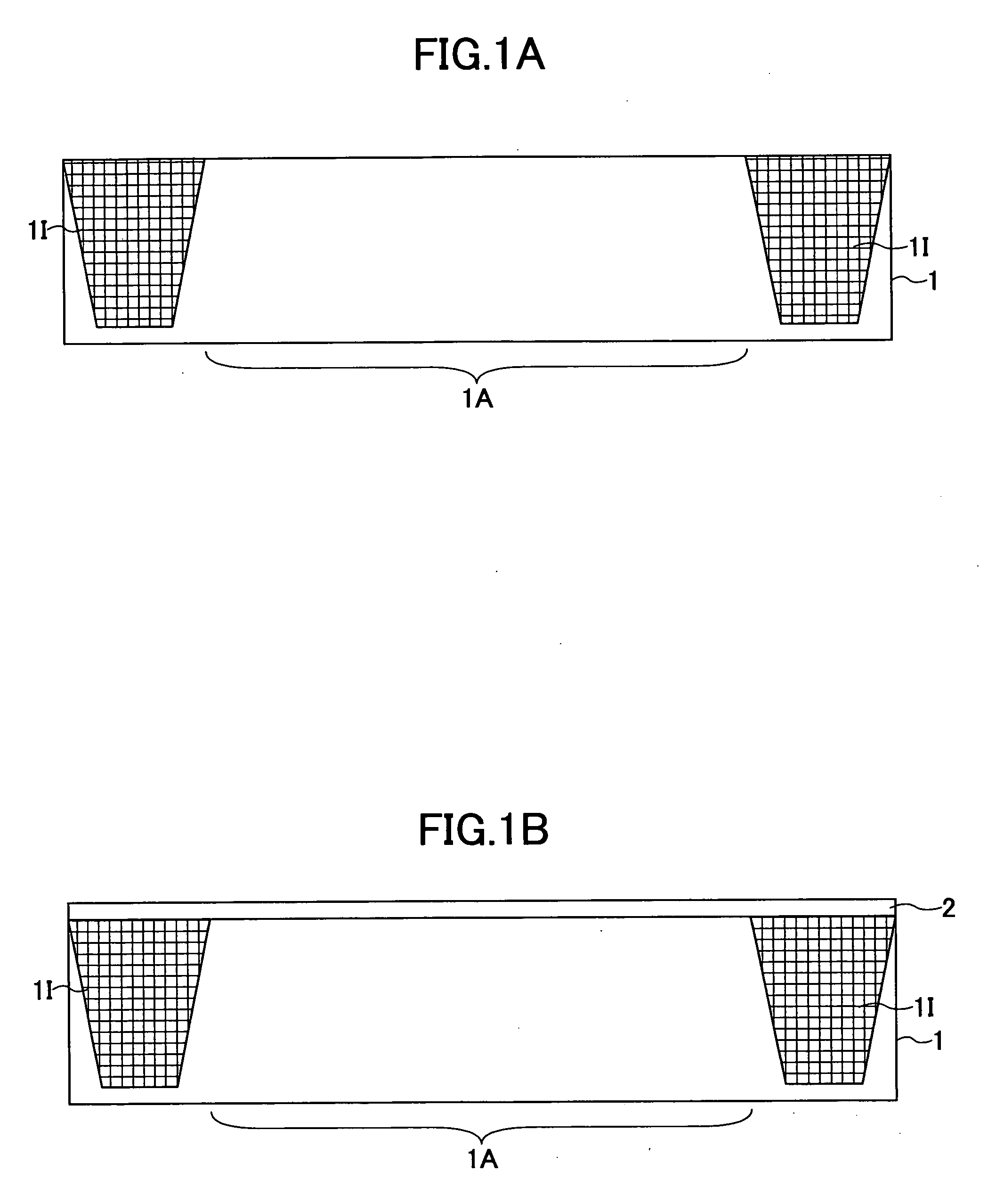
[0045] Referring to FIG. 1A, the semiconductor device 10 is an n-channel MOS transistor formed on a silicon substrate 1, wherein the silicon substrate 1 is formed with a device region 1A by a device isolation region 11 of STI (shallow trench isolation) structure. The device region 1A is formed with a p-type well (not shown), for example.

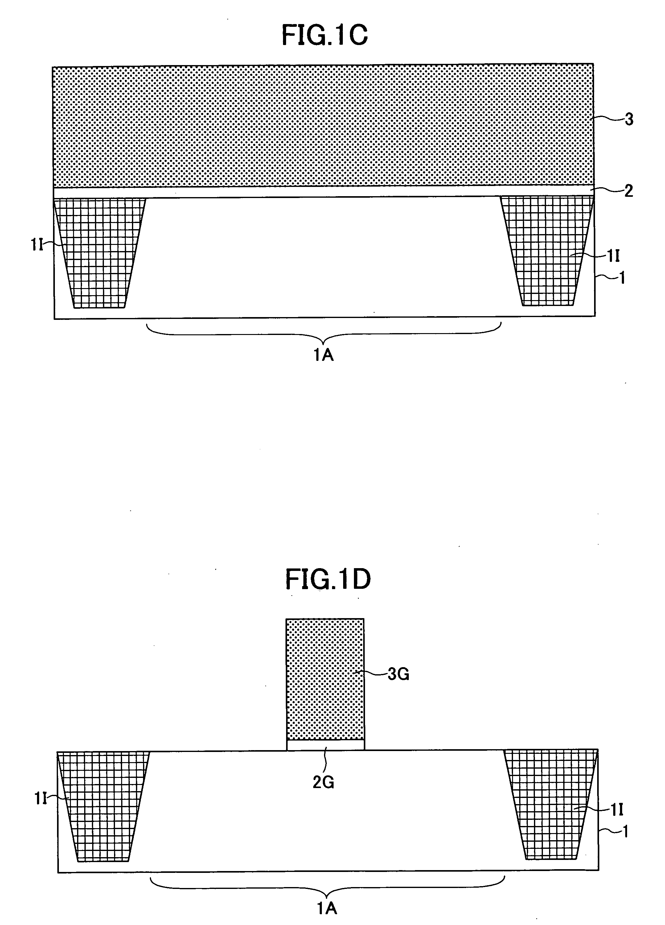
[0046] Next, in the step of FIG. 1B, an SiON film 2 is formed on the silicon substrate 1 with a thickness of 1-2 nm, and a polysilicon film 3 is formed on the SiON film 2 in the step of FIG. 1C typically with a thickness of 100 nm.

[0047] Next, in the step of FIG. 1D, the polysilicon film 3 and the SiON film 2 underneath the polysilicon film 3 are subjected to a patterning process, and there are formed a polysili...

second embodiment

[0075] Next, fabrication process of a CMOS device according to a second embodiment of the present invention will be described with reference to FIGS. 5A-5F.

[0076] Referring to FIG. 5A, a silicon substrate 11 is defined with a device region 11A for an n-channel MOS transistor and a device region 11B for a p-channel MOS transistor by an STI device isolation structure 11I, wherein the device region 11A is doped to p-type and forms a p-type well while the device region 11B is doped to n-type and forms an n-type well. Further, while not illustrated, there is conducted an ion implantation of a p-type impurity element in the device region 11A at a surface part of the silicon substrate 11 for the purpose of threshold control of the n-channel MOS transistor. Similarly, there is conducted an ion implantation of an n-type impurity element in the device region 11B at a surface part of the silicon substrate 11 for the purpose of threshold control of the p-channel MOS transistor.

[0077] On the d...


PUM

PropertyMeasurementUnit
temperatureaaaaaaaaaa
thicknessaaaaaaaaaa
temperatureaaaaaaaaaa

Abstract

A method of fabricating a semiconductor device includes the steps of forming a metallic nickel film on a silicon substrate such that the metallic nickel film covers an insulation film on the silicon substrate and a silicon surface of the silicon substrate, annealing the silicon substrate in a silane gas ambient at a temperature not exceeding 220° C. to form a first nickel silicide layer having a composition primarily of Ni2Si on the silicon surface and a surface of the metallic nickel film, removing the metallic nickel film after the step of forming the nickel silicide layer by a wet etching process, and converting the first nickel silicide layer to a second nickel silicide layer primarily of nickel monosilicide (NiSi) by applying a thermal annealing process.

Description

CROSS-REFERENCE TO RELATED APPLICATION [0001] The present application is based on Japanese priority application No. 2006-008945 filed on Jan. 17, 2006, the entire contents of which are hereby incorporated by reference. BACKGROUND OF THE INVENTION [0002] The present invention generally relates to semiconductor devices and fabrication process thereof, and especially to the fabrication process of a semiconductor device in which a layer of low-resistance nickel silicide, particularly a nickel silicide layer of the NiSi composition is formed on the diffusion region or gate electrode on a semiconductor substrate. [0003] In the art of MOS semiconductor integrated circuit devices, steady progress is being made with regard to improvement of integration density and miniaturization of device size for the purpose of achieving higher operational speed, further diversity of functions, larger memory capacity, further decrease of electric power consumption, or the like. [0004] Today, there is alrea...

Claims


Application Information

Patent Timeline
Patent Type & Authority Applications(United States)
IPC IPC(8): H01L21/4763
CPCH01L29/66636H01L29/7833H01L29/7848H01L21/02068H01L21/28518H01L29/6659H01L21/823814H01L21/823842H01L29/665H01L29/6653H01L21/823807
Inventor UCHINO, YASUNORIKAWAMURA, KAZUOTAMURA, NAOYOSHI
Owner FUJITSU SEMICON LTD
Why Eureka
Try Eureka