

Semiconductor device and method of manufacturing the semiconductor device
a semiconductor and semiconductor technology, applied in the direction of semiconductor devices, semiconductor/solid-state device details, electrical devices, etc., can solve the problems of reducing the heat dissipation efficiency of adjacent members, unable to achieve stable bonding, and disposed between the wedge-bonded portion and the semiconductor element. , to achieve the effect of good heat dissipation and sufficient bonding reliability
- Summary
- Abstract
- Description
- Claims
- Application Information
AI Technical Summary
Benefits of technology
Problems solved by technology
Method used
Image

Examples
first embodiment
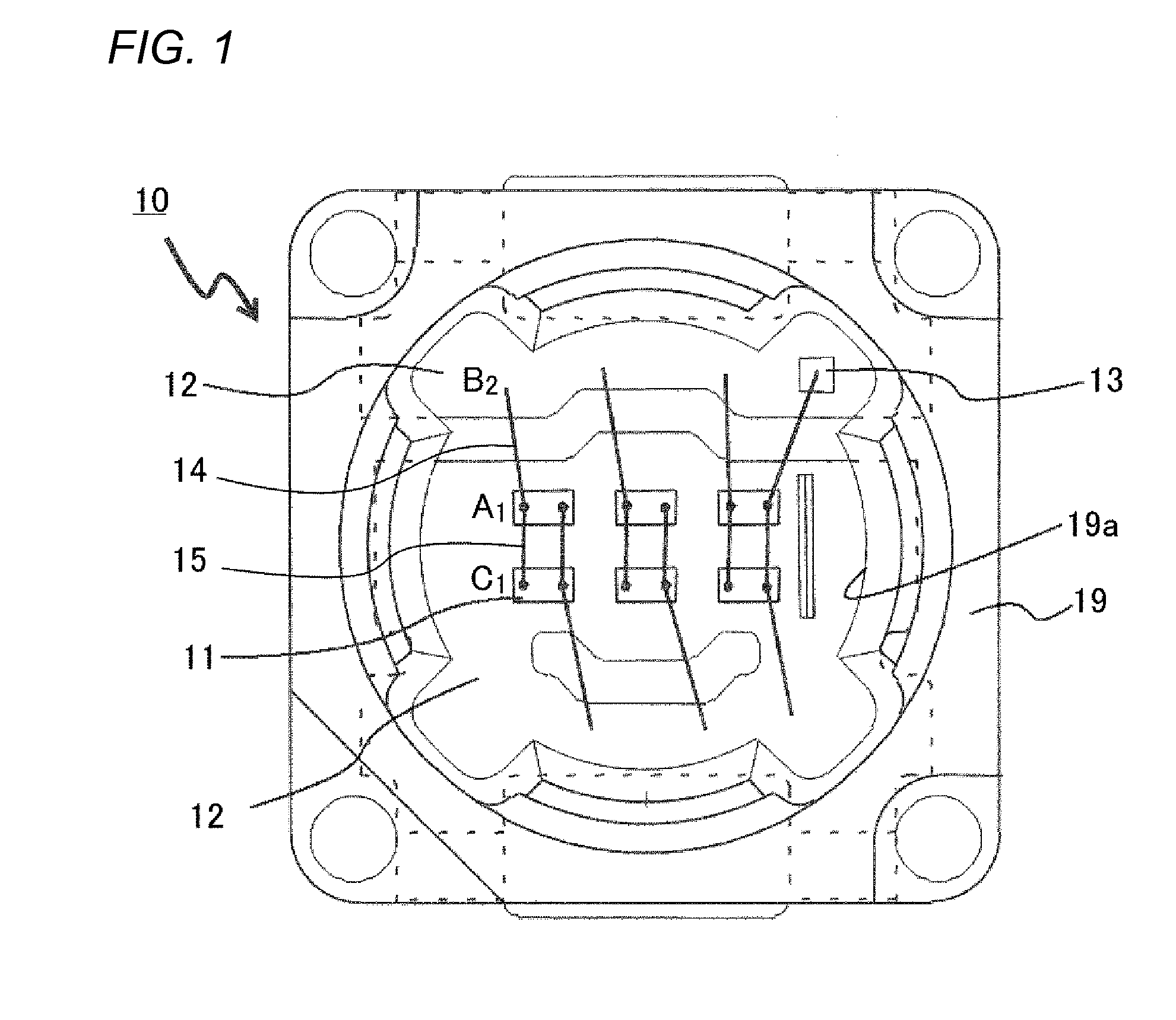
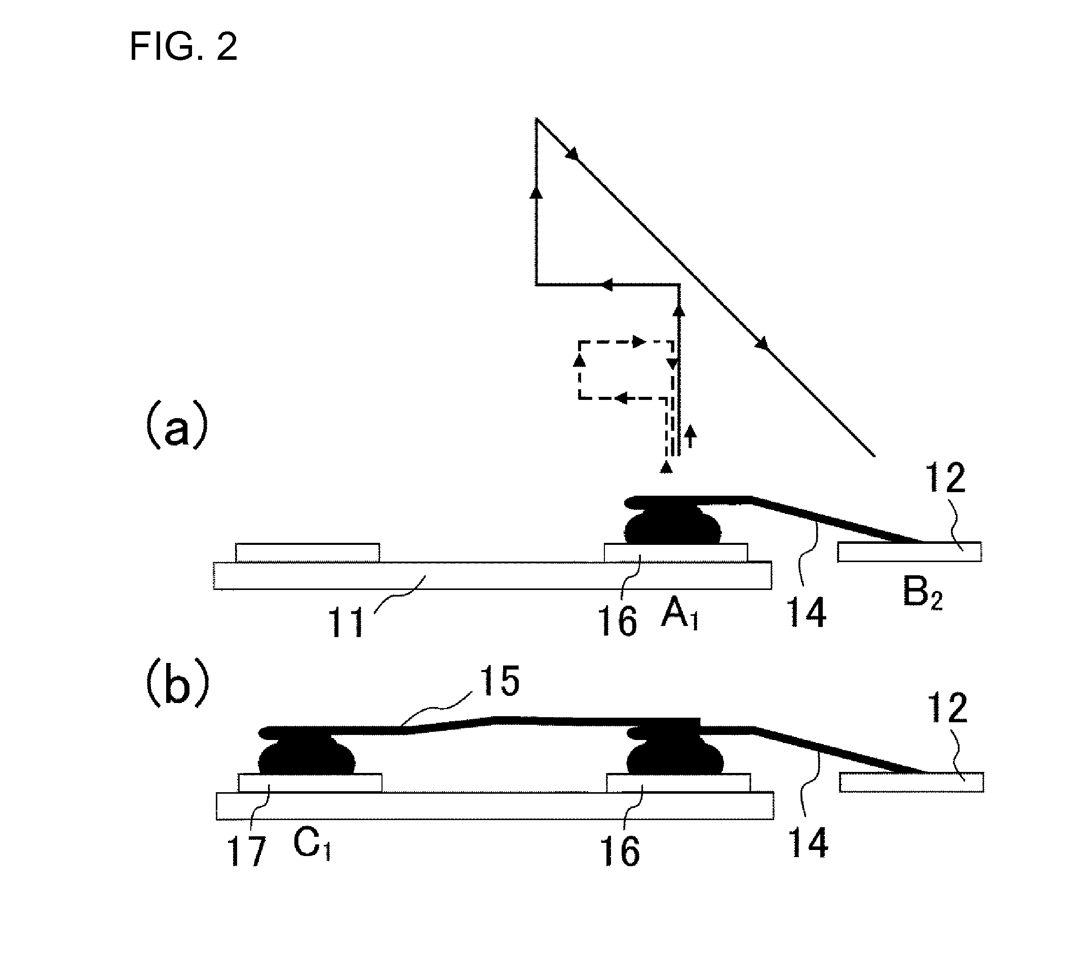
[0027]FIG. 1 is a schematic plan view showing a semiconductor device according to a first embodiment of the present invention. FIG. 2 is a schematic cross-sectional view illustrating a step of wire bonding of a semiconductor device according to a first embodiment of the present invention. FIG. 3A and FIG. 3B are schematic cross-sectional views illustrating wire bonding of a semiconductor device according to a first embodiment of the present invention.
(Semiconductor Device)
[0028]A semiconductor device according to the present embodiment is constituted by at least a semiconductor element 11 and a wire. Moreover, the semiconductor device includes a metal member to which the semiconductor element is mounted and to which a wire is connected, and further includes a sealing resin for holding them integrally. Generally, a wire connects semiconductor elements 11 with each other or a metal member 12 with a semiconductor element 11. A wire includes at least a first wire 14 and a second wire 15...
second embodiment
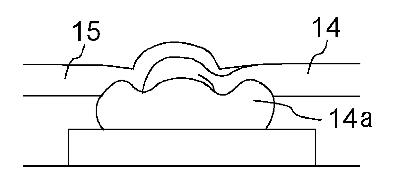
[0059]FIG. 4A and FIG. 4B are schematic cross-sectional views illustrating wire bonding of a semiconductor device according to a second embodiment of the present invention. The semiconductor device according to the second embodiment has different structures in the first wire 14 and the second wire 15 compared with the semiconductor device according to the first embodiment. That is, in the second embodiment, the folded portion 14b of the first wire is in contact with the ball portion 14a. Like members as in the first embodiment are designated by like numerals and their repeated description may be omitted.
[0060]A semiconductor device according to the present embodiment is constituted by at least a semiconductor element and a wire. A wire includes at least a first wire 14 and a second wire 15. In a semiconductor element, a first wire 14 is ball-bonded on an electrode and a second wire 15 is further bonded on the ball-bonded first wire 14. The second wire 15 is bonded to the first wire ...
example 1
[0064]FIG. 1 is a schematic plan view showing a semiconductor device according to a first example of the present invention. FIG. 2 is a schematic cross-sectional view illustrating a step of wire bonding of a semiconductor device according to a first embodiment of the present invention. FIG. 3A and FIG. 3B are schematic cross-sectional views illustrating wire bonding of a semiconductor device according to a first example of the present invention. As shown in FIG. 1, the semiconductor device 10 of the present example is constituted with a semiconductor element (light emitting element) 11, a planar metal member 12, wires electrically connecting between the semiconductor element 11 and the metal member 12 and between the semiconductor elements 11 respectively, and a sealing resin 19 enclosing all the members integrally. The semiconductor device 10 has a reflecting member made of a member capable of reflecting light from the semiconductor element, and a light transmissive member filled i...
PUM
 Abstract
Description
Claims
Application Information