Tape carrier package, individual tape carrier package product, and method of manufacturing the same

a tape carrier and tape carrier technology, applied in semiconductor/solid-state device testing/measurement, semiconductor device details, semiconductor devices, etc., can solve problems such as inability to conduct tests appropriately, and achieve the effect of preventing the interconnection of portions and preventing inappropriate testing

Inactive Publication Date: 2010-11-25
RENESAS ELECTRONICS CORP
View PDF2 Cites 4 Cited by
  • Summary
  • Abstract
  • Description
  • Claims
  • Application Information

AI Technical Summary

Benefits of technology

[0014]According to the present invention, it is possible to prevent the interconnection of the portion intersecting the cutting line from being broken and prevent a test from being conducted inappropriately. The present invention provides a tape carrier package, an individual tape carrier package product, and a method of manufacturing the same.

Problems solved by technology

However, if the narrow portion is provided, the following problems occur.
The narrow portion is broken before a test step in a package state of using a test pad, and the test cannot be conducted appropriately.

Method used


Image

  • Tape carrier package, individual tape carrier package product, and method of manufacturing the same
  • Tape carrier package, individual tape carrier package product, and method of manufacturing the same
  • Tape carrier package, individual tape carrier package product, and method of manufacturing the same

Examples


first embodiment

[0024]FIG. 1 is a plan view of the tape carrier package according to the first embodiment of the present invention.

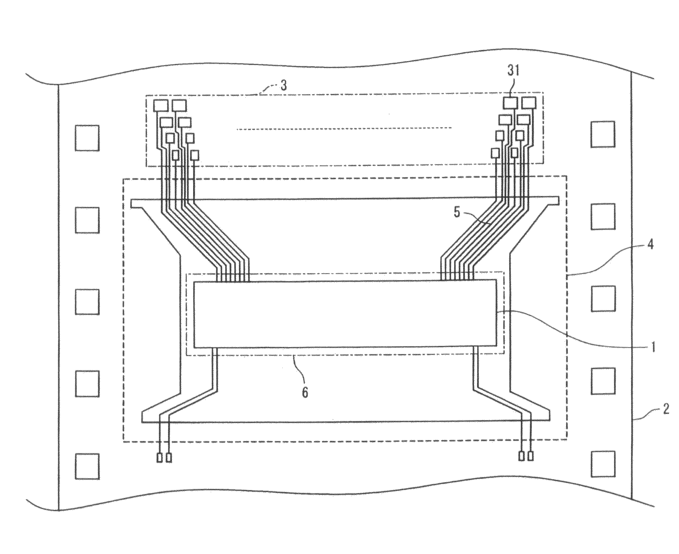
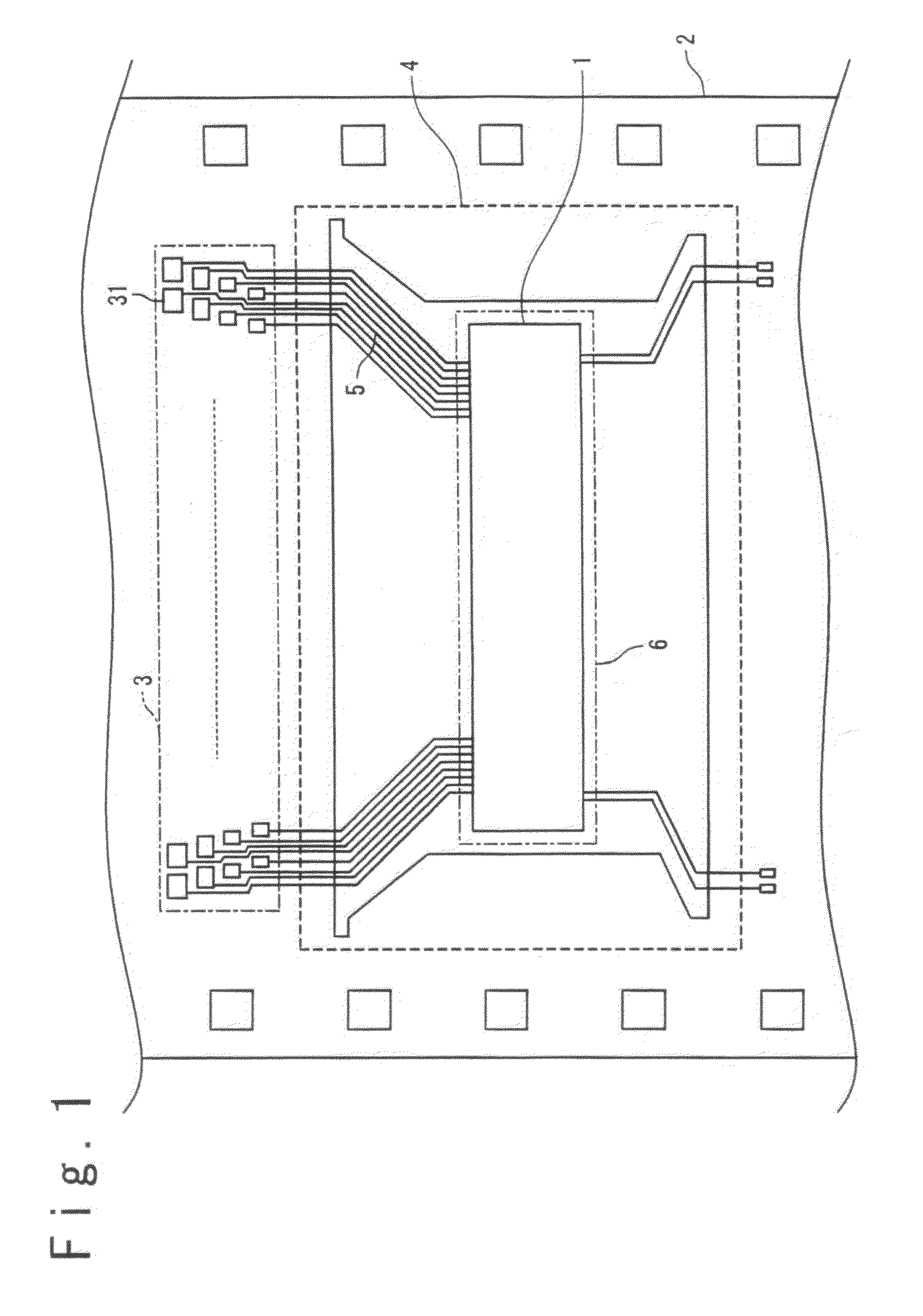
[0025]The tape carrier package according to the first embodiment includes a tape base 2, a semiconductor chip 1, an interconnection group, and a test region 3. Although a plurality of the semiconductor chips 1 are actually mounted on the tape base 2, FIG. 1 shows only one semiconductor chip 1.

[0026]The tape base 2 is made of an insulating resin material or the like. Specifically, polyimide is exemplified as the material of the tape base 2. A chip mount region 6 on which the semiconductor chips 1 are mounted and the test region 3 are provided on the tape base 2. A plurality of test terminals 31 are formed in the test region 3 on the test base 2. The plurality of test terminals 31 are provided to test electric characteristics of the semiconductor chips 1. The interconnection group is formed on the tape base 2. The interconnection group includes a plurality of interconnect...

second embodiment

[0036]A second embodiment of the present invention will next be described. FIG. 4 is a partial enlarged view of the tape carrier package according to the second embodiment. The second embodiment differs from the first embodiment in the number of slits 7. Since the tape carrier package according to the second embodiment is similar to that according to the first embodiment in the other respects, the similar respects will not be described herein in detail.

[0037]As shown in FIG. 4, in the present embodiment, a plurality of (two in FIG. 4) slits 7 are formed in the intersecting portion where one interconnection 5 intersects a cutting line 4.

[0038]The second embodiment can provide similar functions and effects to those of the first embodiment. In addition, by providing a plurality of slits 7, the number of interconnection elements 51 can increase. This can further reduce a probability of breaking the interconnections 5 before a test.

third embodiment

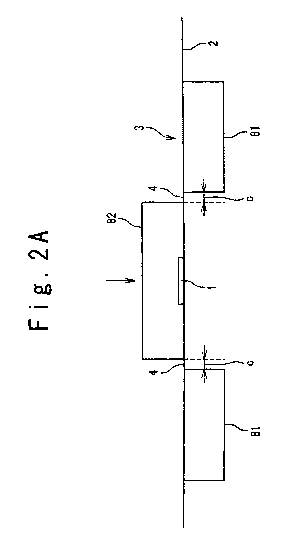
[0039]A third embodiment of the present invention will be described. FIG. 5 is a partial enlarged view of the tape carrier package according to the third embodiment. The third embodiment differs from the preceding embodiments in a shape of the slit 7. Since the tape carrier package according to the third embodiment is similar to those according to the first and second embodiments in the other respects, the similar respects will not be described herein in detail.

[0040]FIG. 5 shows, as a cutting line 4, a center 41 of the cutting line 4, one end 42 of the cutting line 4, and the other end 43 of the cutting line 4. One end 42 of the cutting line 4 is a test region-side end of the cutting line 4 whereas the other end 43 of the cutting line 4 is a semiconductor chip-side end of the cutting line 4.

[0041]As shown in FIG. 5, each slit 7 is provided to be narrower as being closer to the semiconductor chip-side. By providing each slit 7 in such a manner, each interconnection element 51 is thi...


PUM


Abstract

A tape carrier package includes: a tape base; and interconnections formed on the tape base and extending to intersect a cutting line. At least a slit is formed along each of the interconnections, to intersect the cutting line and to divide the interconnection into a plurality of interconnection elements.

Description

INCORPORATION BY REFERENCE[0001]This patent application claims a priority on convention based on Japanese Patent Application No. 2009-124539 filed on May 22, 2009. The disclosure thereof is incorporated herein by reference.TECHNICAL FIELD[0002]The present invention relates to a tape carrier package, an individual tape carrier package product, and a method of manufacturing the same.BACKGROUND ART[0003]There is known a TCP (Tape Carrier Package). It is assumed that types of TCPs include a so-called COF (Chip On Film) package. The TCP has a structure in which a semiconductor chip is mounted on an insulating tape base. Because of use of the tape base, the TCP can be made thin and used in various purposes such as a LCD driver device.[0004]In the TCP, a plurality of semiconductor chips are mounted on one tape base. Thereinafter, the tape base is cut off along a predetermined cutting line, thereby obtaining a plurality of individual products. In the specification of the present application...

Claims


Application Information

Patent Timeline
Patent Type & Authority Applications(United States)
IPC IPC(8): H01L23/544H01L21/78H01L23/498
CPCH01L22/32H01L23/4985H01L23/544H01L2223/54426H01L2223/54473H01L2924/0002H01L2223/54486H01L2924/00
Inventor YOSHINO, ISAO
Owner RENESAS ELECTRONICS CORP
Why Eureka
Try Eureka