Organic electroluminescence display device

a display device and electroluminescent technology, applied in semiconductor devices, electrical devices, instruments, etc., can solve the problems of difficult control of the gap between the device substrate and the sealing substrate, contamination of organic el materials, and defects in images, so as to prevent defective products and increase production yields

Inactive Publication Date: 2010-11-25
HITACHI DISPLAYS +1
View PDF4 Cites 59 Cited by
  • Summary
  • Abstract
  • Description
  • Claims
  • Application Information

AI Technical Summary

Benefits of technology

[0028]In the solid sealed organic electroluminescence (EL) display device according to the present invention, it is possible to detect the presence of a pinhole in the interfacial surface of the inorganic passivation film at an early stage. This makes it possible to prevent the defective product in which the pinhole is present, from being delivered to the market. Further, by detecting the pinhole at an early stage, it is possible to detect a problem of CVD or other processes at an early stage. As a result, the production yield can be increased.
[0029]Further, in the present invention, the presence of the pinhole in the inorganic passivation film is detected by the color exhibition of the pigment added to the organic flattening film. In this case, when the color exhibition of the pigment can return to transparent, the inorganic passivation film can be formed again after the removal of the water in the organic EL display device. In this way, it is possible to reproduce the organic EL display device with no pinhole.

Problems solved by technology

The dark spot grows as the time passes, causing a defect in an image.
However, the hollow sealed organic EL display device has the following problems.
It is difficult to control the gap between the device substrate and the sealing substrate.
The organic EL material is contaminated by the gas emitted from a sealant for sealing the organic EL display device.
The throughput of the organic EL display device is low.
There is also a problem with the completed organic EL display device that when an external force is applied to the device substrate or the sealing substrate, the device substrate and the sealing substrate come into contact with each other, causing the organic EL layer to be destroyed.
The defect occurs after the delivery of the product as a defect in the market, resulting in the loss of the trust of the customers.
However, the pinhole is very small and is difficult to be found even with a microscope.
It may not be possible to find the pinhole of the passivation film on the device substrate in which an active matrix circuit pattern, organic EL layer, and the like, are formed.
As described above, the conventional technology may not typically be able to find the defect in the passivation film that is likely to cause a defect in the market.

Method used


Image

  • Organic electroluminescence display device
  • Organic electroluminescence display device
  • Organic electroluminescence display device

Examples


first embodiment

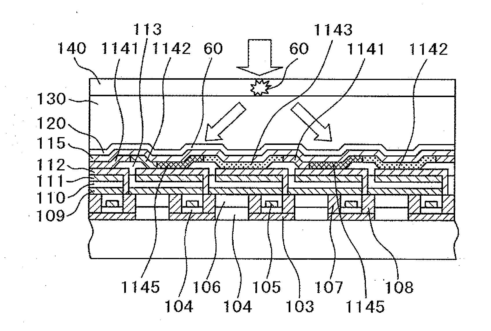
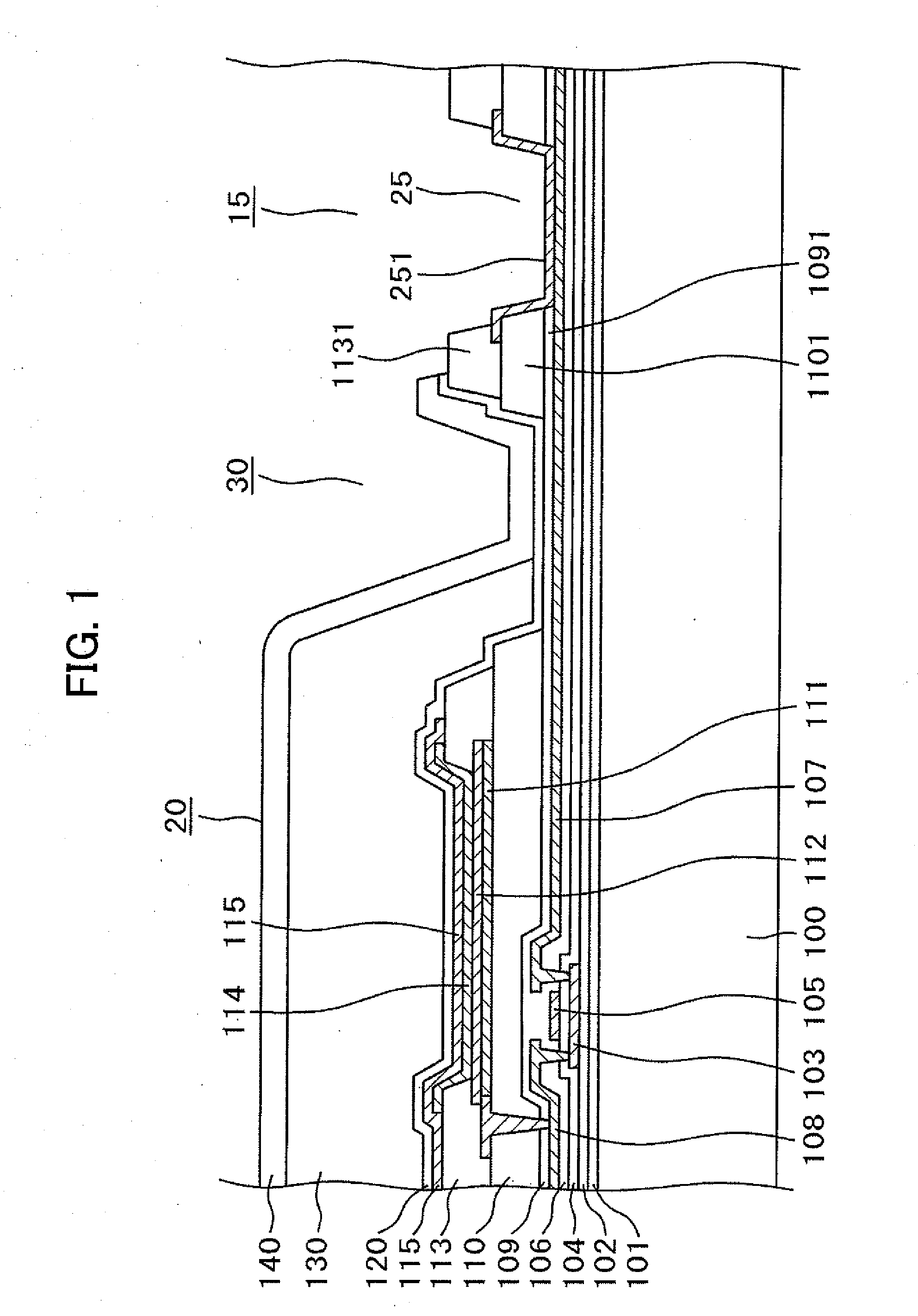
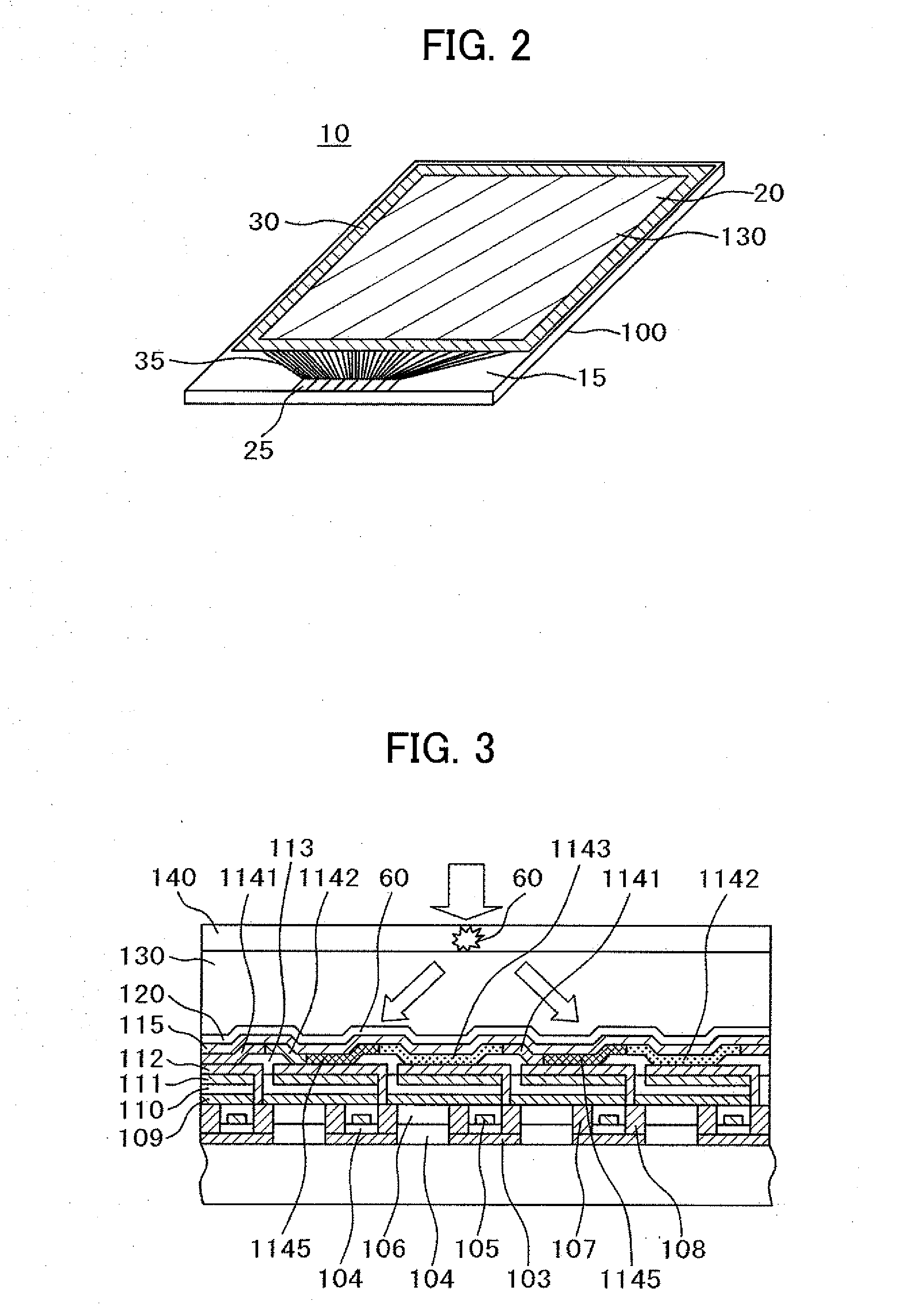
[0039]FIG. 2 is a perspective view of an organic EL display device 10 to which the present invention is applied. In FIG. 2, a display area 20 and a terminal area 15 are formed on a device substrate 100 of glass. The display area 20 is covered by an organic flattening film 130. The organic flattening film 130 and the display area 20 are substantially equal to each other. A peripheral sealing area 30, which is covered by an inorganic passivation film, is formed in the periphery of the display area 20 in which the organic flattening film 130 is not present. The organic film is permeable to the water, so that the organic flattening film 130 is removed in the peripheral sealing area 30.

[0040]The terminal area 15 is formed on the outside of the display area 20. In the terminal area 15, leader lines 35 of scan lines, image signal lines, and power lines are formed and connected to a terminal portion 25 of the terminal area 15. Scan signals, image signals, power, and the like, are supplied f...

second embodiment

[0074]FIG. 7 shows a second embodiment. The second embodiment is different from the first embodiment in that the organic EL layer 114 is protected from water by a laminate film 50, instead of using the organic flattening film 130. In FIG. 7, the second inorganic passivation film 120 is formed on the upper electrode 115 of the organic EL layer 114, which is the same as the configuration of the first embodiment. However, in the second embodiment, the laminate film 50 is formed on the second inorganic passivation film 120. Then, the third inorganic passivation film 140 is formed on the laminate film 50. The laminate film 50 includes a laminate film base material 51 and a thermoplastic adhesive material 52.

[0075]The third inorganic passivation film 140 is formed on the laminate film 50. At this time, an SiN film of about 1 μm is applied by a low temperature CVD. The surface of the laminate film 50 is very flat with few bubbles or other defects. The number of defects in the third inorgan...

third embodiment

[0078]FIG. 8 is a cross-sectional view showing a third embodiment of the present invention. FIG. 8 is a cross-sectional view, similar to FIG. 1, from the end portion of the display area 20, to the peripheral sealing area 30 and the terminal area 15. In FIG. 8, the second inorganic passivation film 120 is formed on the upper electrode 115 of the organic EL display 114, which is the same as the first embodiment. In the third embodiment, the laminate film 50 described in the second embodiment is laminated on the second inorganic passivation film 120. Further, in the third embodiment, a barrier layer 53 for blocking water is provided by co-depositing alumina and silica on a surface of the laminate film base material 51. Then, the third inorganic passivation film 140 is formed on the barrier layer 53 by a low temperature CVD.

[0079]As described above, in this embodiment, the barrier layer 53 is provided on the surface of the laminate film 50, so that little water is transmitted through th...


PUM


Abstract

A solid-sealed organic electroluminescence display device is provided with means of preventing the occurrence of a dark spot in the market, due to the degradation of an organic EL light emitting layer by water entering from a pinhole of a sealant. In order to prevent the degradation of the organic EL layer by water, a first inorganic film, an organic flattening film, and a second inorganic film are formed on an upper electrode. Water entering from the pinhole in the second inorganic film diffuses into the organic flattening film, and degrades the organic EL layer in several months, resulting in a defect in the market. In order to prevent this, a material capable of reacting with oxygen or water and exhibiting color is added to the organic flattening film. Then, the defective organic electroluminescence display device is picked up and eliminated prior to delivery to the market.

Description

CLAIM OF PRIORITY[0001]The present application claims priority from Japanese Patent Application JP 2009-121669 filed on May 20, 2009, the content of which is hereby incorporated by reference into this application.FIELD OF THE INVENTION[0002]The present invention relates to an organic electroluminescence display device, and more particularly to a highly reliable organic electroluminescence display device capable of suppressing an occurrence of a dark spot or other defects caused by water.BACKGROUND OF THE INVENTION[0003]In an organic electroluminescence (EL) display device, an organic EL layer interposed between a lower electrode and an upper electrode. The light emission of the organic EL layer of the organic EL display device is controlled by applying a certain voltage to the upper electrode, and by applying a data signal voltage to the lower electrode. The data signal voltage is supplied to the lower electrode through a thin film transistor (TFT). The organic EL layer emits light ...

Claims


Application Information

Patent Timeline
Patent Type & Authority Applications(United States)
IPC IPC(8): G09G3/30
CPCH01L51/5237H01L27/3244H10K59/12H10K50/846H10K50/8445
Inventor TANAKA, MASAHIRO
Owner HITACHI DISPLAYS
Why Eureka
Try Eureka