SRAM and method for accessing SRAM

a static random access memory and access method technology, applied in the field of sram and access method, can solve the problems of variable static random access memory, inability to ignore precharge voltage variation, and inability to solve the variation above precharge voltage, so as to improve the snm in the static random access memory and achieve high accuracy

Inactive Publication Date: 2010-11-25
RENESAS ELECTRONICS CORP
View PDF1 Cites 19 Cited by
  • Summary
  • Abstract
  • Description
  • Claims
  • Application Information

AI Technical Summary

Benefits of technology

[0022]According to the present invention, an SNM in the static random access memory can be improved with high accuracy.

Problems solved by technology

However, in the static random access memory operating at the power supply voltage as low as approximately 1.0 V, a variation of the static random access memory due to a variation in the precharge voltage cannot be ignored.
However, a method for generating the precharge voltage is not disclosed, and therefore the above precharge voltage variation has not been solved.

Method used


Image

  • SRAM and method for accessing SRAM
  • SRAM and method for accessing SRAM
  • SRAM and method for accessing SRAM

Examples


first embodiment

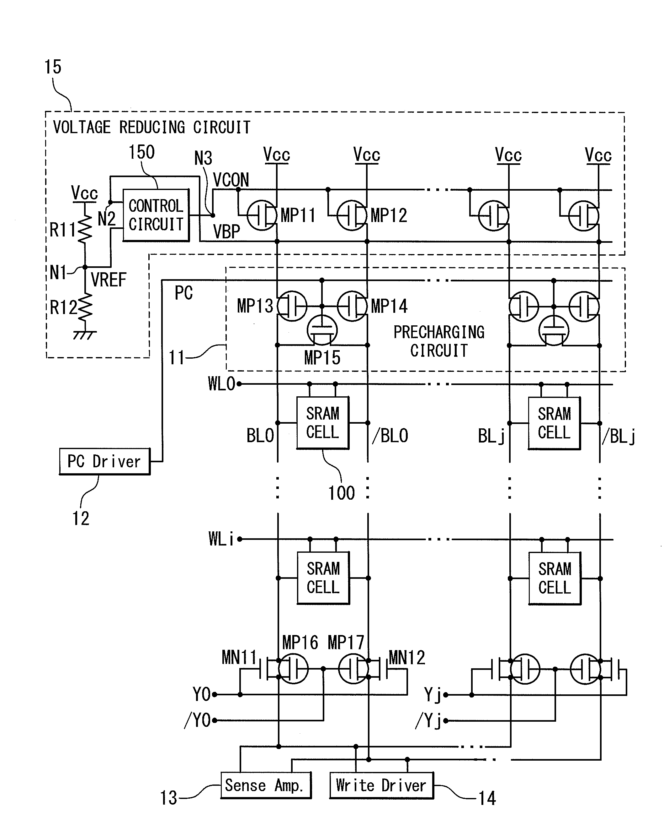
[0039]Referring to FIGS. 4 to 9, the SRAM according to a first embodiment of the present invention will be described.

[0040]FIG. 4 is a diagram illustrating a configuration of the SRAM according to the first embodiment of the present invention. The SRAM in the first embodiment includes a plurality of memory cells (SRAM cells) 100, a precharge circuit 11, a precharge driver 12, a sense amplifier 13, a write driver 14, and a voltage reducing circuit 15. The plurality of memory cells 100 are arranged in a matrix and are connected to a plurality of word lines WL0 to WLi and a plurality of pairs of bit lines BL0 and / BL0 to BLj and / BLj.

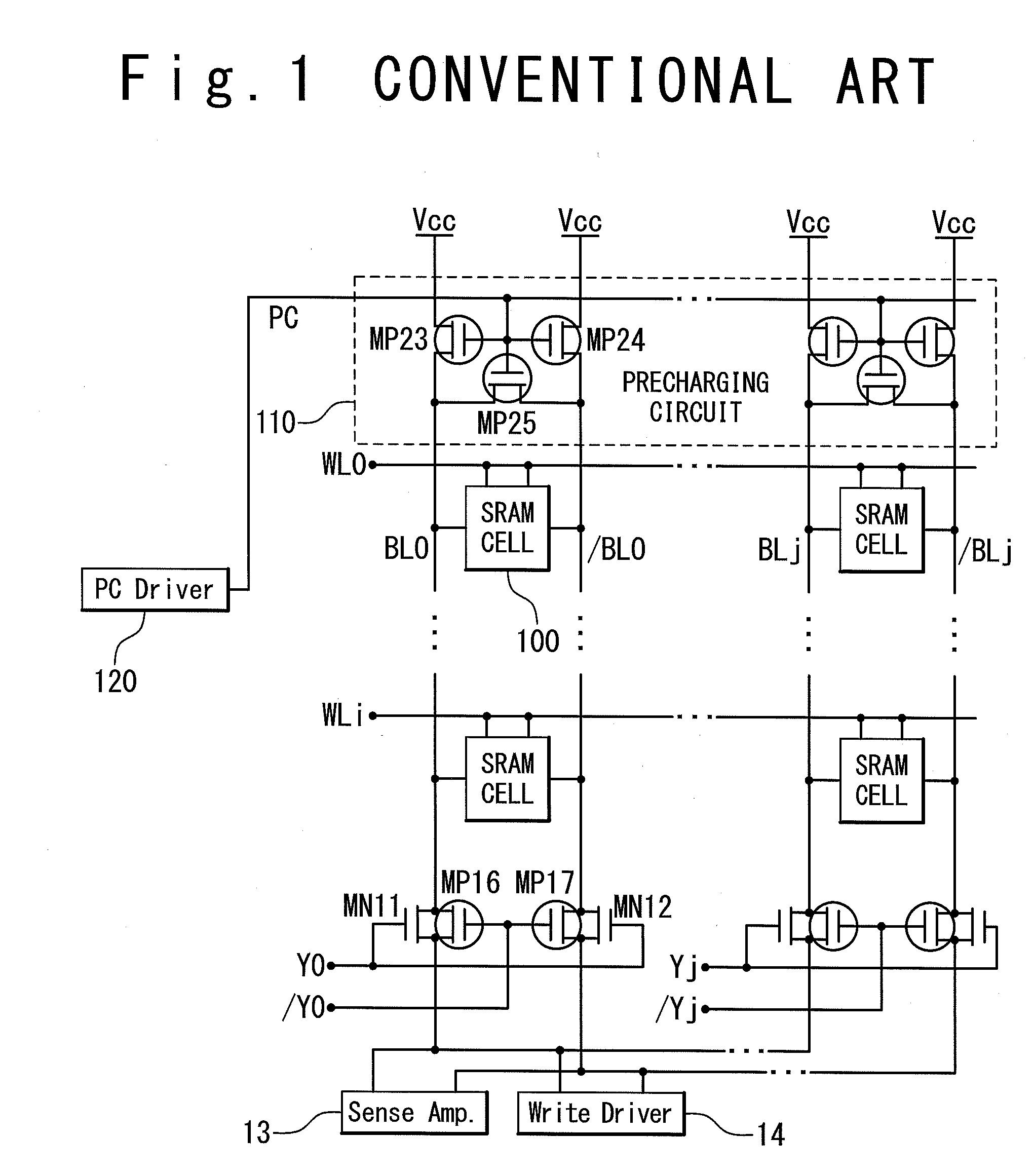
[0041]The precharge circuit 11, the precharge driver 12, the sense amplifier 13, the write driver 14, and the voltage reducing circuit 15 are connected to the plurality of pairs of bit lines BL0 and / BL0 to BLj and / BLj. In the following, the memory cell 100 connected to the word line WL0 and the pair of bit lines BL0 and / BL0 will be described. The other ...

second embodiment

[0068]Referring to FIGS. 10 to 13, the SRAM according to a second embodiment of the present invention will be described.

[0069]FIG. 10 is a diagram illustrating a configuration of the SRAM according to the second embodiment of the present invention. The second embodiment is different from the first embodiment in the configurations and operations of the voltage reducing circuit and the precharge driver. The other configurations and operations are the same. In the following, details of the SRAM in the second embodiment will be described in terms of the differences from the first embodiment.

[0070]The SRAM in the second embodiment is provided with a precharge driver 17 that outputs a first precharge control signal PC and a second precharge control signal φPC; and a voltage reducing circuit 16 that changes the precharge voltage VBP in response to the second precharge control signal φPC.

[0071]The voltage reducing circuit 16 is provided with a control circuit 160 illustrated in FIG. 11 in p...


PUM


Abstract

A static random access memory includes: a memory cell connected with a pair of bit lines and supplied with a power supply voltage from a first power supply; a precharge circuit connected with the pair of bit lines and configured to precharge the pair of bit lines with a precharge voltage; and a voltage reducing circuit connected between the precharge circuit and the first power supply. The voltage reducing circuit includes: a control circuit comprising a differential amplifier circuit which is configured to amplify a difference input of a reference voltage generated through resistance division of the power supply voltage and the precharge voltage supplied to a node to output a control signal; and a voltage reduction control transistor connected between the node and the first power supply and configured to generate the precharge voltage in response to the control signal. The precharge circuit includes: precharge transistors connected between the bit lines and the node and configured to control supply of the precharge voltage to the bit lines in response to a first precharge control signal.

Description

INCORPORATION BY REFERENCE[0001]This patent application claims a priority on convention based on Japanese Patent Application No. 2009-120676 filed on May 19, 2009. The disclosure thereof is incorporated herein by reference.TECHNICAL FIELD[0002]The present invention relates to an SRAM (static random access memory) and a method for accessing an SRAM, and more particularly, to an SRAM in which bit lines are precharged before accessing a memory cell.BACKGROUND ART[0003]In order to improve data reading and writing speeds, there is known a technique for precharging bit lines connected to a memory cell before accessing the memory cell.[0004]FIG. 1 is a diagram illustrating a configuration of a conventional SRAM. Referring to FIG. 1, the conventional SRAM includes a plurality of memory cells (SRAM cells) 100 respectively connected to a plurality of word lines WL0 to WLi and a plurality of pairs of bit lines BL0 and / BL0 to BLj and / BLj. A precharge circuit 110 is connected between a power s...

Claims


Application Information

Patent Timeline
Patent Type & Authority Applications(United States)
IPC IPC(8): G11C7/00G11C5/14G11C7/02
CPCG11C11/413G11C7/12
Inventor KOBAYASHI, YASUO
Owner RENESAS ELECTRONICS CORP
Why Eureka
Try Eureka