Light emission device and display device using the same

a technology of light emission device and display device, which is applied in the manufacture of electric discharge tubes/lamps, electric discharge tubes, cold cathodes, etc., can solve the problems of inefficient electric field generated between the gate electrode and the cathode electrode, and achieve the effect of improving electron emission characteristics, efficient generating electric fields, and increasing electron emission

Inactive Publication Date: 2010-12-02
SAMSUNG SDI CO LTD
View PDF3 Cites 0 Cited by
  • Summary
  • Abstract
  • Description
  • Claims
  • Application Information

AI Technical Summary

Benefits of technology

[0011]Aspects of embodiments of the present invention are directed toward a light emission device having improved electron emission characteristics (e.g., increased emission of electrons) by efficiently generating an electric field, and a display device using the same.

Problems solved by technology

However, when the cathode electrode is flattened, the electric field generated between the gate electrode and the cathode electrode is not efficient.

Method used


Image

  • Light emission device and display device using the same
  • Light emission device and display device using the same
  • Light emission device and display device using the same

Examples


first embodiment

[0035]Hereinafter, referring to FIGS. 1 to 3, a light emission device 101 will be described.

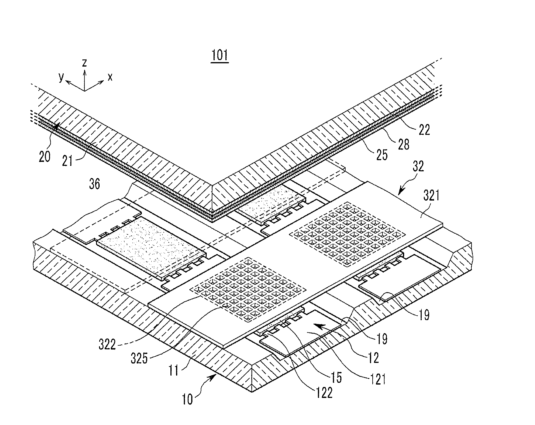
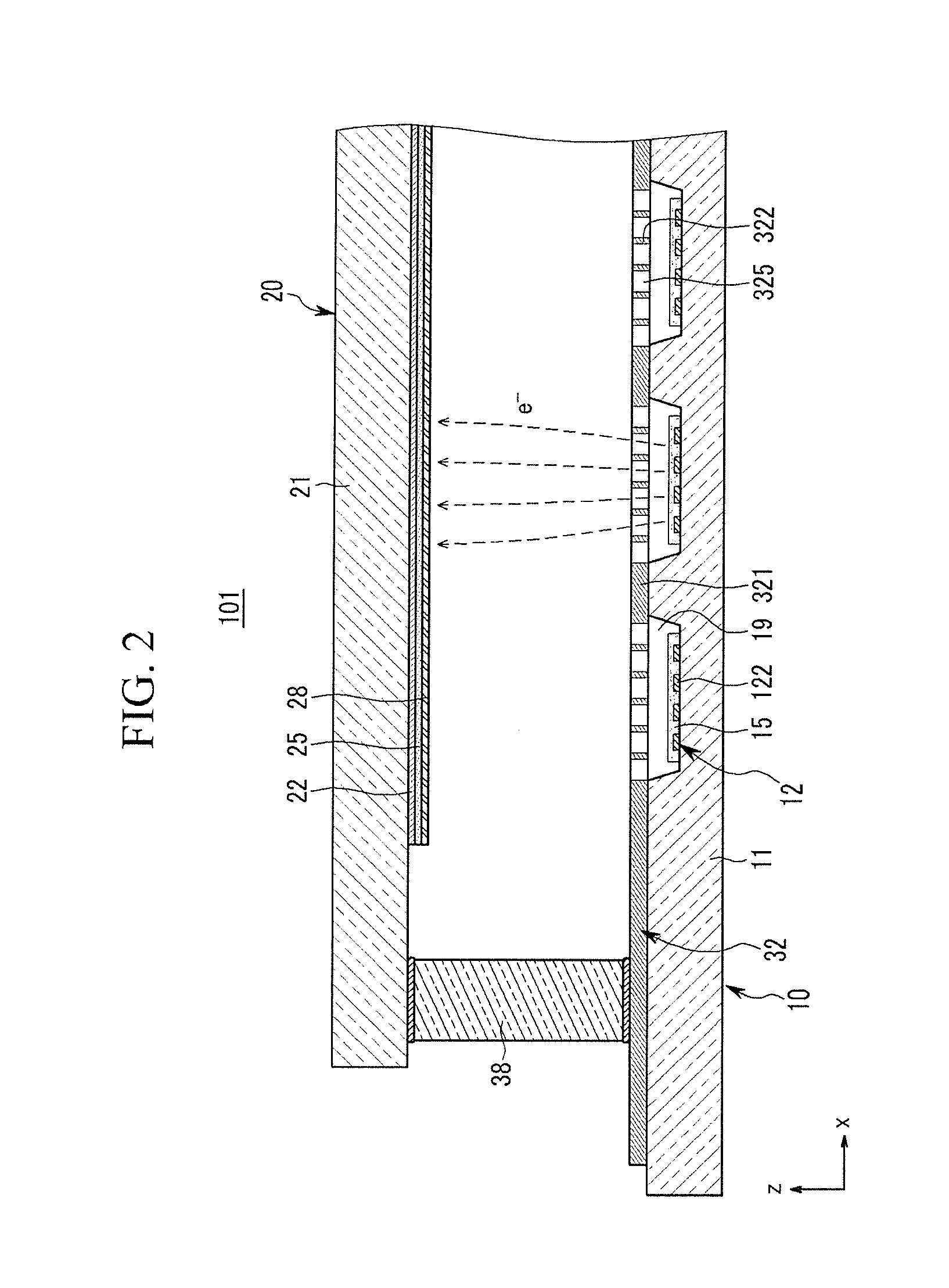
[0036]As shown in FIG. 1, the light emission device 101 includes a first substrate assembly 10, a second substrate assembly 20 facing the first substrate assembly 10, and a sealing member 38 (shown in FIG. 2) that is disposed at edges (edge portions) of the first substrate assembly 10 and the second substrate assembly 20 to bond and seal the two substrate assemblies 10 and 20 to each other. The inner space formed by the first substrate assembly 10, the second substrate assembly 20, and the sealing member 38 is evacuated to be in a vacuum state maintained at a vacuum degree of about 10−6 Torr.

[0037]The first substrate assembly 10 includes a substrate or substrate body (hereinafter, referred to as “first substrate body 11”), a first electrode 12, an electron emission unit (emission region) 15, and a second electrode 32. Here, the first electrode 12 is a cathode electrode (cathode) and the seco...

second embodiment

[0066]Hereinafter, referring to FIG. 4, a light emission device will be described.

[0067]As shown in FIG. 4, in the second embodiment, a first electrode 13 of the light emission device includes (or only includes) single line parts 131 positioned at both ends of the first electrode 13, respectively, and a branch line part 132 connecting both single line parts 131. Further, in one embodiment, an electron emission unit 16 formed just above the branch line part 132 of the first electrode 13 is formed to have a stripe pattern to extend along the branch line part 132 of the first electrode 13 such that the electron emission unit 16 extends through a region crossing the second electrode 32 (shown in FIG. 1) and regions not crossing the second electrode 32.

[0068]By this configuration, the light emission device 101 can further facilitate a process of arranging the first electrode 13 and the second electrode 32 with each other (without an extra alignment) while increasing or maximizing emissi...


PUM


Abstract

A light emission device includes a substrate body having a concave portion extending along a first direction within the substrate body; a first electrode within the concave portion and extending along the first direction, the first electrode having a portion separated into a plurality of separate parts, the plurality of separate parts being parallel to each other; a second electrode on a front surface of the substrate body and extending along a second direction crossing the first electrode; and an electron emission unit on the first electrode and spaced apart from the second electrode.

Description

CROSS-REFERENCE TO RELATED APPLICATION[0001]This application claims priority to and the benefit of Korean Patent Application No. 10-2009-0046034, filed in the Korean Intellectual Property Office on May 26, 2009, the entire content of which is incorporated herein by reference.BACKGROUND[0002]1. Field[0003]The following description relates to a light emission device and a display device using the same, and more particularly, to a light emission device using a field emission effect and a display device using the same.[0004]2. Description of Related Art[0005]A light emission device can emit light and include a light emission device using a field emission effect. A light emission device using the field emission effect can include a light emission device that includes a front substrate formed with a phosphor layer (or a fluorescent layer) and an anode electrode (anode), and a rear substrate formed with electron emission regions and driving electrodes. Here, edges (edge portions) of the fr...

Claims


Application Information

Patent Timeline
Patent Type & Authority Applications(United States)
IPC IPC(8): H01J1/02
CPCH01J29/04H01J31/127H01J29/467H01J1/30
Inventor YUN, BOK-CHUN
Owner SAMSUNG SDI CO LTD
Why Eureka
Try Eureka