Plasma processing apparatus

Inactive Publication Date: 2010-12-09
TOKYO ELECTRON LTD
View PDF9 Cites 15 Cited by
  • Summary
  • Abstract
  • Description
  • Claims
  • Application Information

AI Technical Summary

Benefits of technology

[0020]According to the present invention, in the plasma processing apparatus provided with the plane antenna having a plurality of slots, the second waveguide(s) is provided in the conductive member (cover) disposed over the plane antenna such that it covers the plane antenna. The provision of the second waveguide(s) can adjust and equalize the distribution of electric field in a flat waveguide constituted by the plane antenna and the conductive member. Consequently, the coefficient of reflection (reflected waves)

Problems solved by technology

Further, when processing conditions are changed in a plasma processing apparatus, a plasma in a processing chamber is likely to become unstable or uneven.
In addition, especially when a large-sized

Method used


Image

  • Plasma processing apparatus
  • Plasma processing apparatus
  • Plasma processing apparatus

Examples


first embodiment

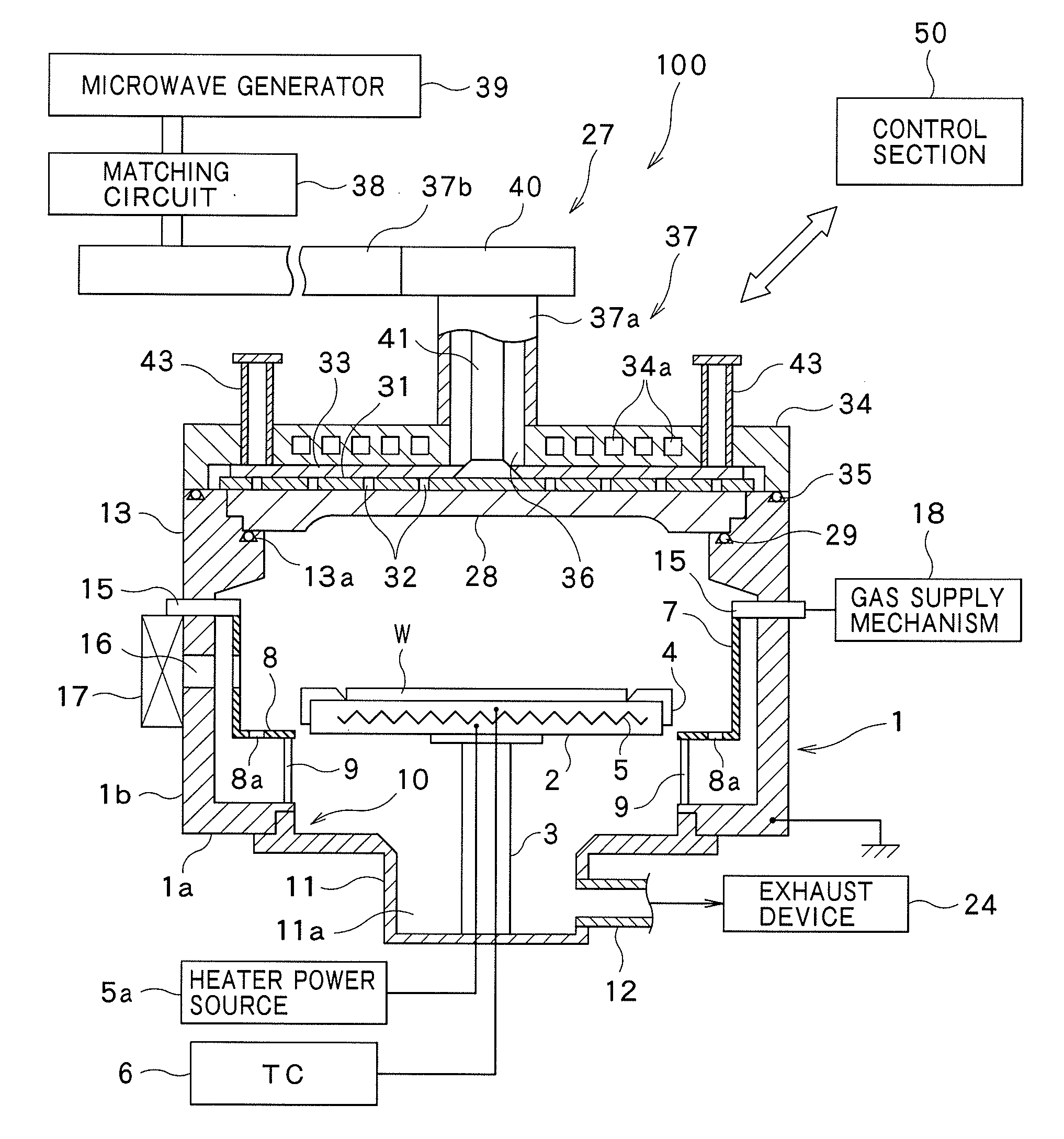
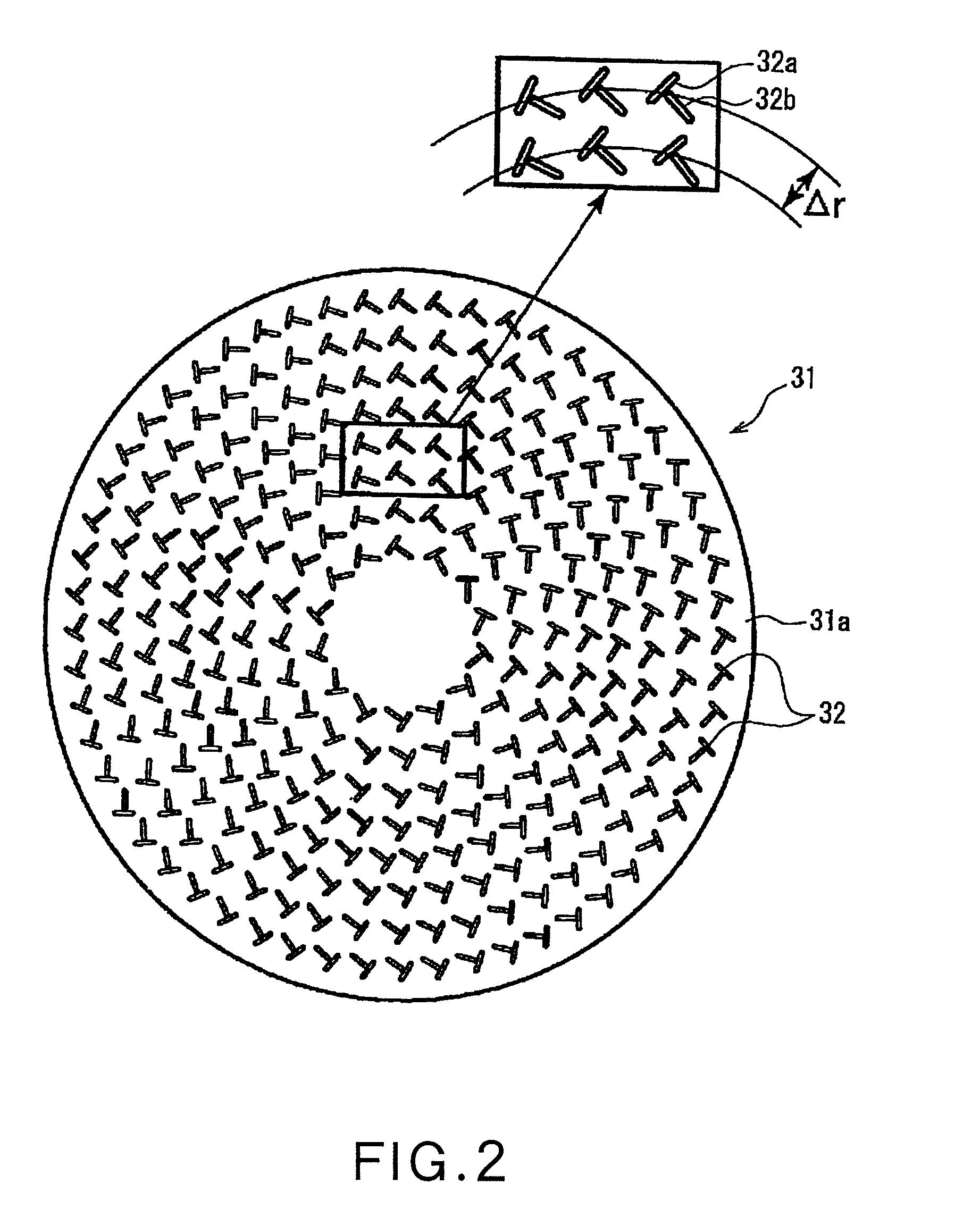
[0053]Preferred embodiments of the present invention will now be described in detail with reference to the drawings. FIG. 1 is a cross-sectional view schematically showing the construction of a plasma processing apparatus 100 according to a first embodiment of the present invention. FIG. 2 is a plan view showing the plane antenna of the plasma processing apparatus 100 of FIG. 1. FIG. 3 is a perspective view illustrating the schematic construction of the top portion of the plasma processing apparatus 100 of FIG. 1. FIG. 4 is a diagram illustrating the schematic construction of the control system of the plasma processing apparatus 100 of FIG. 1.

[0054]The plasma processing apparatus 100 is constructed as a plasma processing apparatus capable of generating a high-density, low-electron temperature, microwave-excited plasma by introducing microwaves into a processing chamber by means of a plane antenna having a plurality of slot-like holes, in particular an RLSA (radial line slot antenna)...

experimental examples

[0170]An experiment was conducted to verify the fact that processing uniformity can be enhanced by adjusting the height of a stub(s). The method and results of the experiment will now be described.

[0171]A plasma processing apparatus which was used in the experiment is first described with reference to FIG. 28.

[0172]The plasma processing apparatus shown in FIG. 28 differs from the plasma processing apparatus shown in FIG. 1 only in the following respects: First, a protrusion 28a is provided in the center of the lower surface of the transmissive plate 28. Further, instead of the cover ring 4, a cover 4a which covers the entire upper surface of the stage 2 is provided. Positioning of a wafer W is performed by means of a guide 4b provided on the upper surface of the cover 4a. Instead of the stub(s) 43, four stubs 43A, each capable of changing the effective stub height, are provided. A movable body 43a is provided in the interior of each stub 43A; and the movable body 43a can be moved ve...


PUM

PropertyMeasurementUnit
Timeaaaaaaaaaa
Electrical conductoraaaaaaaaaa
Areaaaaaaaaaaa

Abstract

A microwave plasma processing apparatus (100) of a slot antenna type includes a plane antenna plate (31) constituting a flat waveguide and a cover (34) of a conductive member. The cover (34) is provided with a stub (43) as a second waveguide for adjusting electric field-distribution in the flat waveguide. The stub (43) is provided in the cover (34) of the conductive member. In plan view, the stub (43) is arranged to overlap slots (32) constituting a slot pair arranged at the outermost circumference of the plane antenna plate (31). By appropriately arranging the stub, it is possible to control electric field-distribution in the flat waveguide thereby to generate a uniform plasma.

Description

TECHNICAL FIELD[0001]The present invention relates to a plasma processing apparatus for processing a processing object with a plasma generated by introducing microwaves into a processing container by means of a plane antenna having slots.BACKGROUND ART[0002]As a plasma processing apparatus for carrying out plasma processing, such as oxidation or nitridation, of a processing object such as a semiconductor wafer, an apparatus is known which generates a plasma in a processing chamber by introducing microwaves having a predetermined frequency, for example 2.45 GHz, into the processing chamber by using a slot antenna (see e.g. Japanese Patent Laid-Open Publications Nos. 11-260594 and 2001-223171). Such a microwave plasma processing apparatus is capable of forming a surface wave plasma having a high plasma density.[0003]With reference to such a slot antenna-type plasma processing apparatus, the distribution of plasma is likely to somewhat differ even among the same apparatuses of the same...

Claims


Application Information

Patent Timeline
IPC IPC(8): H01L21/306
CPCH01J37/32192H05H1/46H01J37/32229H01J37/3222
Inventor OTA, RYOSAKUADACHI, HIKARUNAKANISHI, TOSHIOUEDA, ATSUSHIKANG, SONGYUNMOROZ, PAULVENTZEK, PETER
Owner TOKYO ELECTRON LTD
Why Eureka
Try Eureka