Apparatus for large area plasma processing

a large-area plasma and apparatus technology, applied in electrical apparatus, semiconductor/solid-state device manufacturing, electric discharge tubes, etc., can solve the problems of difficult to obtain a large-area plasma processing with a high processing rate and a uniform processing distribution, film thickness control, and film property control produced by conventional pecvd devices becoming more problematic, so as to enhance the excitation of helicon-like waves and uniform processing distribution.

Active Publication Date: 2019-03-26
HELYSSEN
View PDF18 Cites 0 Cited by
  • Summary
  • Abstract
  • Description
  • Claims
  • Application Information

AI Technical Summary

Benefits of technology

[0004]Documents EP 0 949 352 B1 and U.S. Pat. No. 6,363,881 B2 disclose a planar ladder-shaped antenna for Plasma Enhanced Chemical Vapor Deposition. The ladder-shaped antenna has an upper side conductive bar, a lower side conductive bar, and several parallel conductive bars joining the upper and lower conductive bars. A power distributor with a plurality of electrical wires is used for uniformly distributing a high-frequency power to the ladder-shaped antenna, making it possible to obtain a better film thickness distribution.
[0020]Considering that the plasma quickly diffuses from areas with high current intensities to areas with lower current intensities, a more uniform distribution of plasma can be created by the antenna of the invention.
[0031]With such a magnetic field, plane polarized helicon-like waves can be excited in the plasma, so that the processing rate of the apparatus is improved.
[0040]Furthermore, the travelling current distribution enhances strongly the helicon-like waves excitation.

Problems solved by technology

But, even with a power distributor, it remains very difficult to obtain a large area plasma processing with a high processing rate and a uniform processing distribution.
As the size of substrates continues to grow, film thickness control and film property control produced by conventional PECVD devices become more problematical.

Method used


Image

  • Apparatus for large area plasma processing
  • Apparatus for large area plasma processing
  • Apparatus for large area plasma processing

Examples


Embodiment Construction

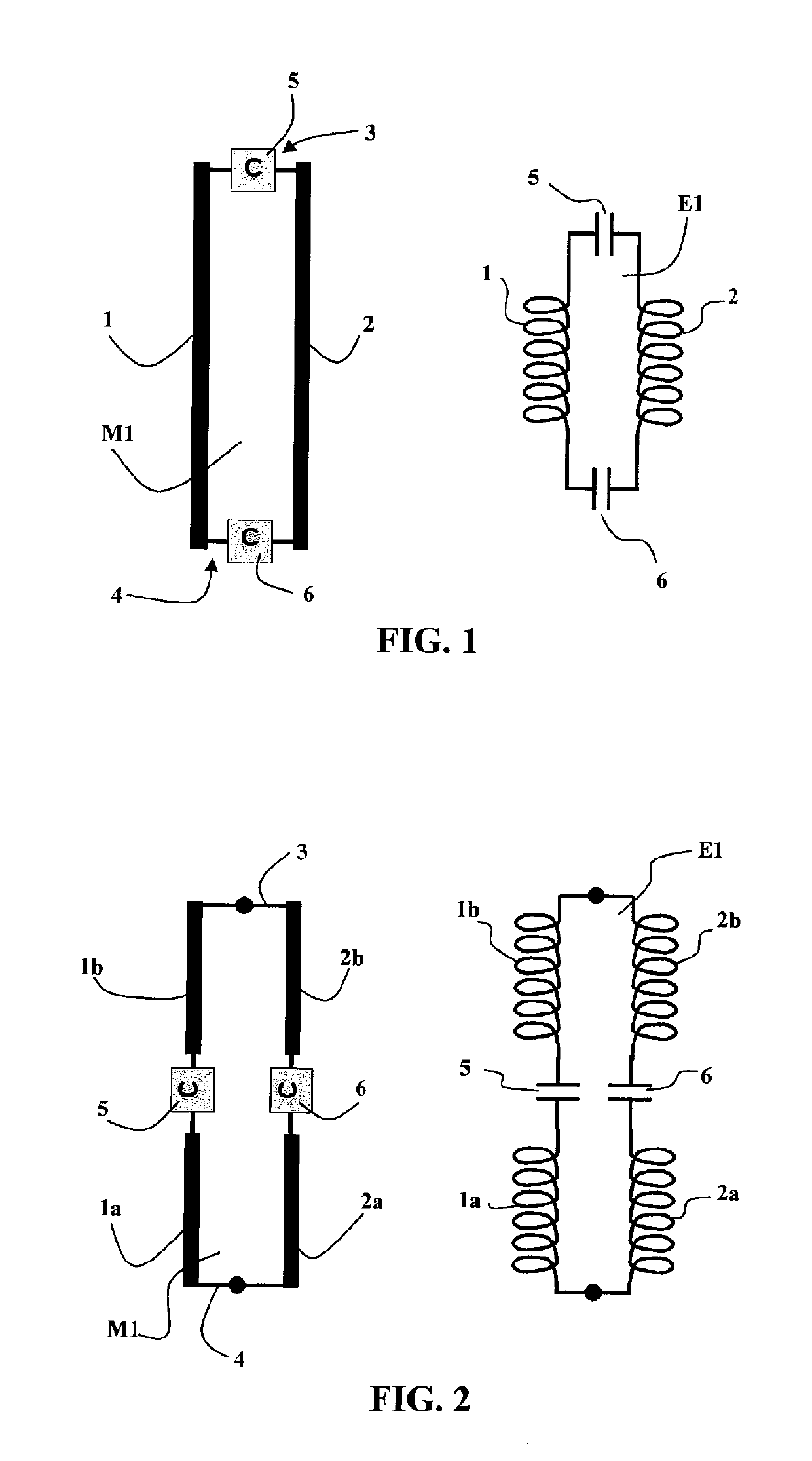
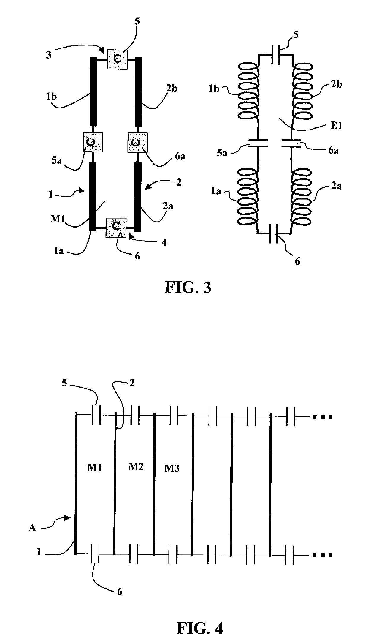
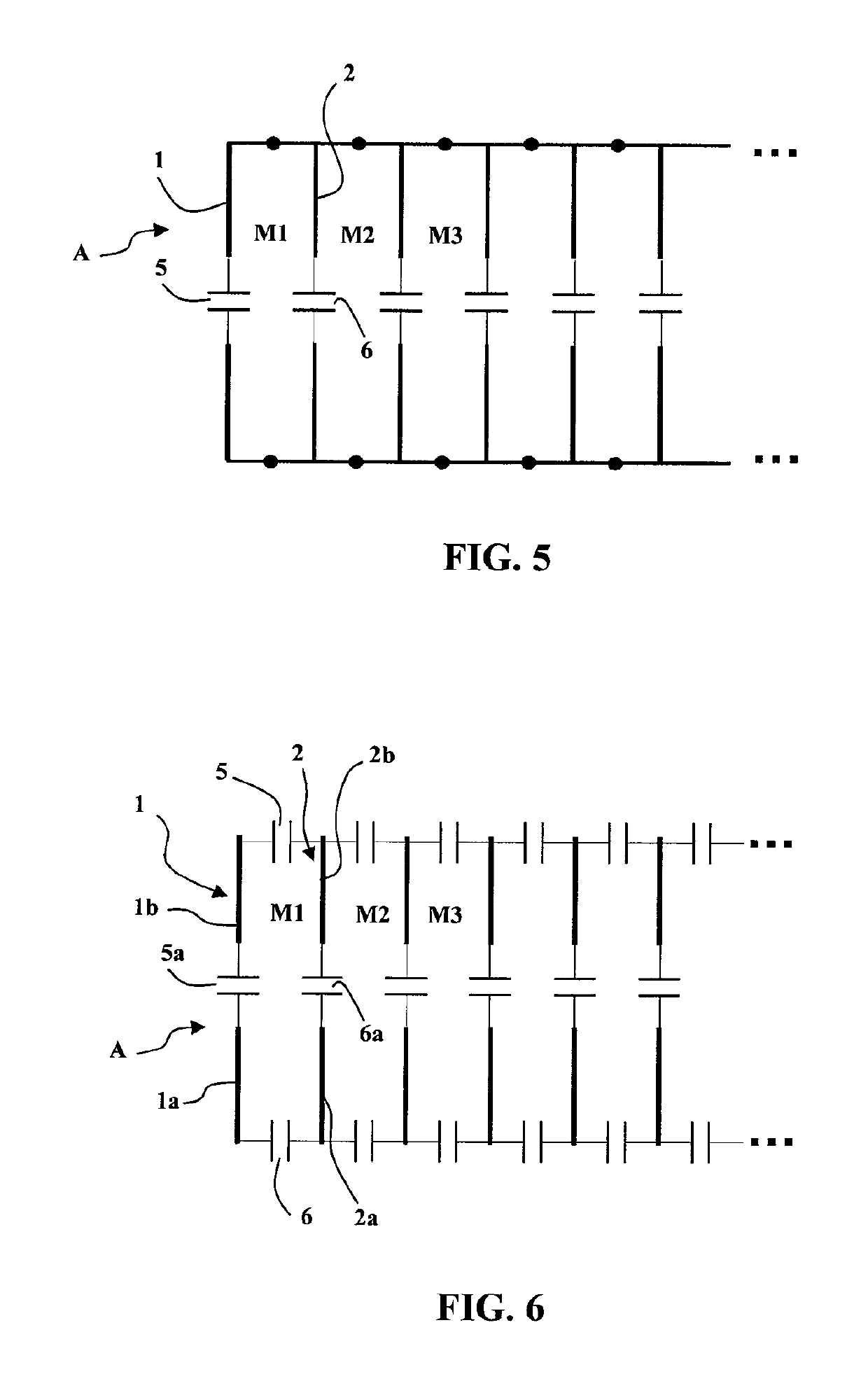
[0060]According to the invention, a plane antenna with a plurality of elementary resonant meshes is provided as a source for generating large area plasmas.

[0061]FIGS. 1, 2 and 3 show three embodiments for such an elementary mesh M1, and the corresponding equivalent electric circuit E1.

[0062]Each elementary mesh M1 has two parallel longer conductive legs 1 and 2 whose ends are interconnected by transverse shorter connecting elements 3 and 4.

[0063]The longer connecting legs 1 and 2 act essentially as inductive components. Each elementary mesh has at least two opposing capacitors 5 and 6.

[0064]In the high pass mesh of FIG. 1, the opposing capacitors 5 and 6 constitute said shorter connecting elements 3 and 4.

[0065]In the low pass mesh of FIG. 2, the opposing capacitors 5 and 6 are each connected in series between two lengths 1a, 1b or 2a, 2b of a respective conductive leg 1 or 2.

[0066]In the pass band mesh of FIG. 3, two first opposing capacitors 5 and 6 constitute said shorter connect...


PUM

PropertyMeasurementUnit
sizeaaaaaaaaaa
sizeaaaaaaaaaa
diameteraaaaaaaaaa

Abstract

An apparatus for large area plasma processing according to the invention comprises at least one plane antenna (A) having a plurality of interconnected elementary resonant meshes (M1, M2, M3), each mesh (M1, M2, M3) comprising at least two conductive legs (1, 2) and at least two capacitors (5, 6). A radiofrequency generator excites said antenna (A) to at least one of its resonant frequencies. A process chamber is in proximity of said antenna (A). Said antenna (A) produces an electromagnetic field pattern with a very well defined spatial structure, which allows a great control on the excitation of the plasma.

Description

TECHNICAL FIELD OF THE INVENTION[0001]The present invention relates to an apparatus for large area plasma processing improving uniformity and plasma density.SUMMARY OF THE INVENTION[0002]Plasma processing is used very frequently for various applications such as surface coating, manufacturing flat panels or solar cells. Plasma processing comprises etching process, deposition process, surface modification, surface functionalization. For example, Plasma Enhanced Chemical Vapor Deposition (PECVD) is generally used to deposit thin films on a substrate, such as a transparent substrate for flat panel display, or a semiconductor wafer.[0003]PECVD is generally accomplished by introducing a precursor gas or gas mixture into a vacuum chamber that contains a substrate. The precursor gas or gas mixture is typically directed downwardly through a distribution plate situated near the top of the chamber. The precursor gas or gas mixture in the chamber is energized into a plasma generated by a plasma...

Claims


Application Information

Patent Timeline
Patent Type & Authority Patents(United States)
IPC IPC(8): H01J37/32
CPCH01J37/321H01J37/3211H01J37/3222H01J37/32284H01J37/32256
Inventor GUITTIENNE, PHILIPPE
Owner HELYSSEN
Why Eureka
Try Eureka