Semiconductor device and electrostatic discharge protection method for the semiconductor device

a technology for semiconductor devices and shielding films, applied in emergency protective circuits, emergency protective arrangements for limiting excess voltage/current, electric devices, etc., can solve the problem of low tolerance of thin gate insulating films against electrostatic charges, and achieve high electrostatic discharge protection performance

Inactive Publication Date: 2010-12-09
RENESAS ELECTRONICS CORP
View PDF5 Cites 8 Cited by
  • Summary
  • Abstract
  • Description
  • Claims
  • Application Information

AI Technical Summary

Benefits of technology

[0013]According to the present invention, a secondary protection circuit releases a surge electric current in response to a trigger signal for suppressing a surge voltage applied to a region near a semiconductor integrated circuit at an early timing. As a result, a semiconductor device and an electrostatic discharge protection method for the semiconductor device having a high electrostatic discharge protection performance are provided.

Problems solved by technology

However, there is a problem that the tolerance of a thin gate insulating-film against electrostatic charges is low.

Method used


Image

  • Semiconductor device and electrostatic discharge protection method for the semiconductor device
  • Semiconductor device and electrostatic discharge protection method for the semiconductor device
  • Semiconductor device and electrostatic discharge protection method for the semiconductor device

Examples


Embodiment Construction

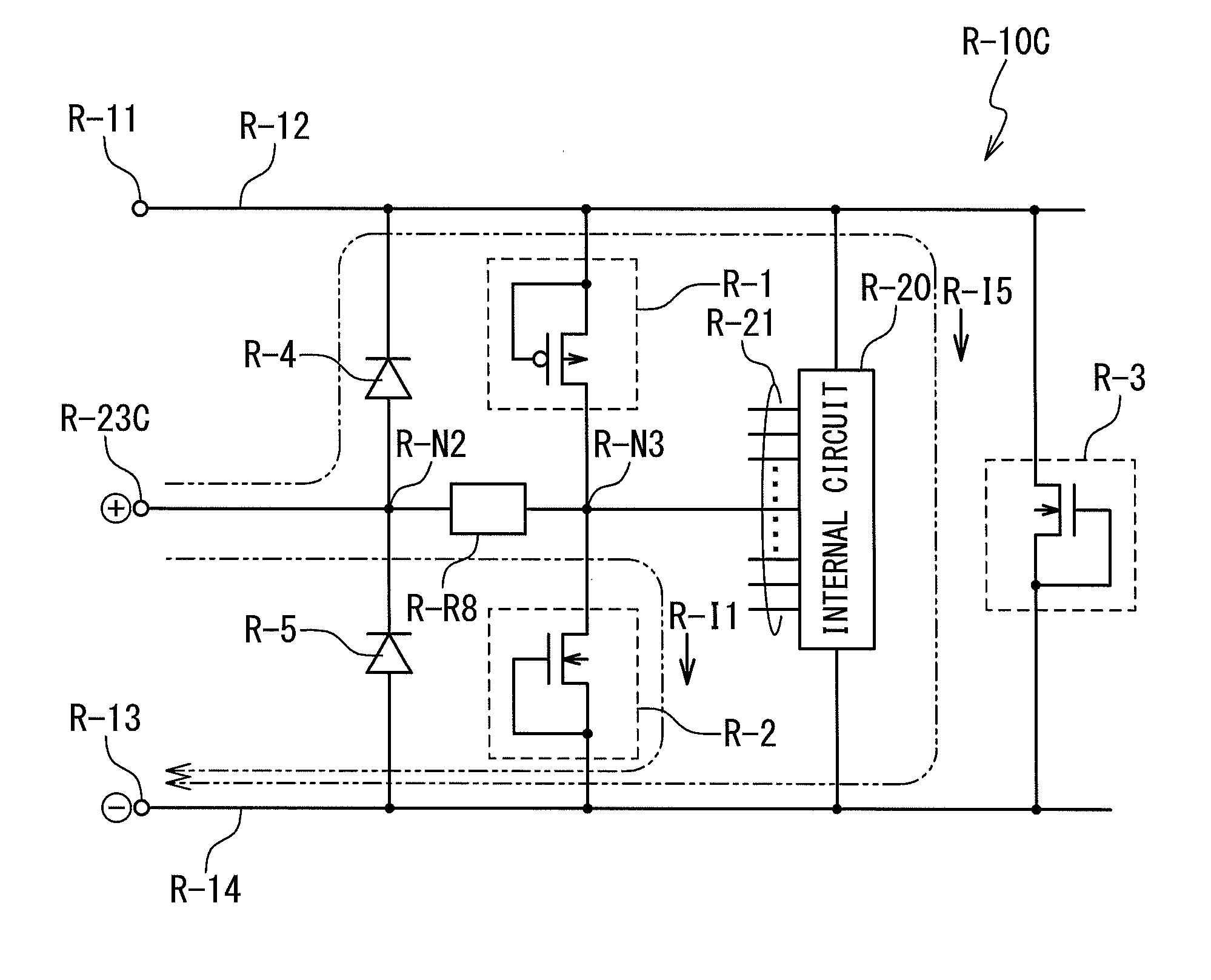
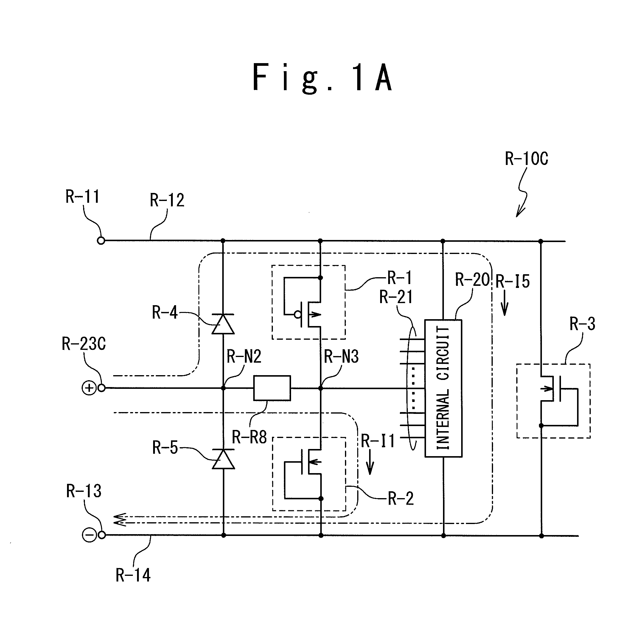
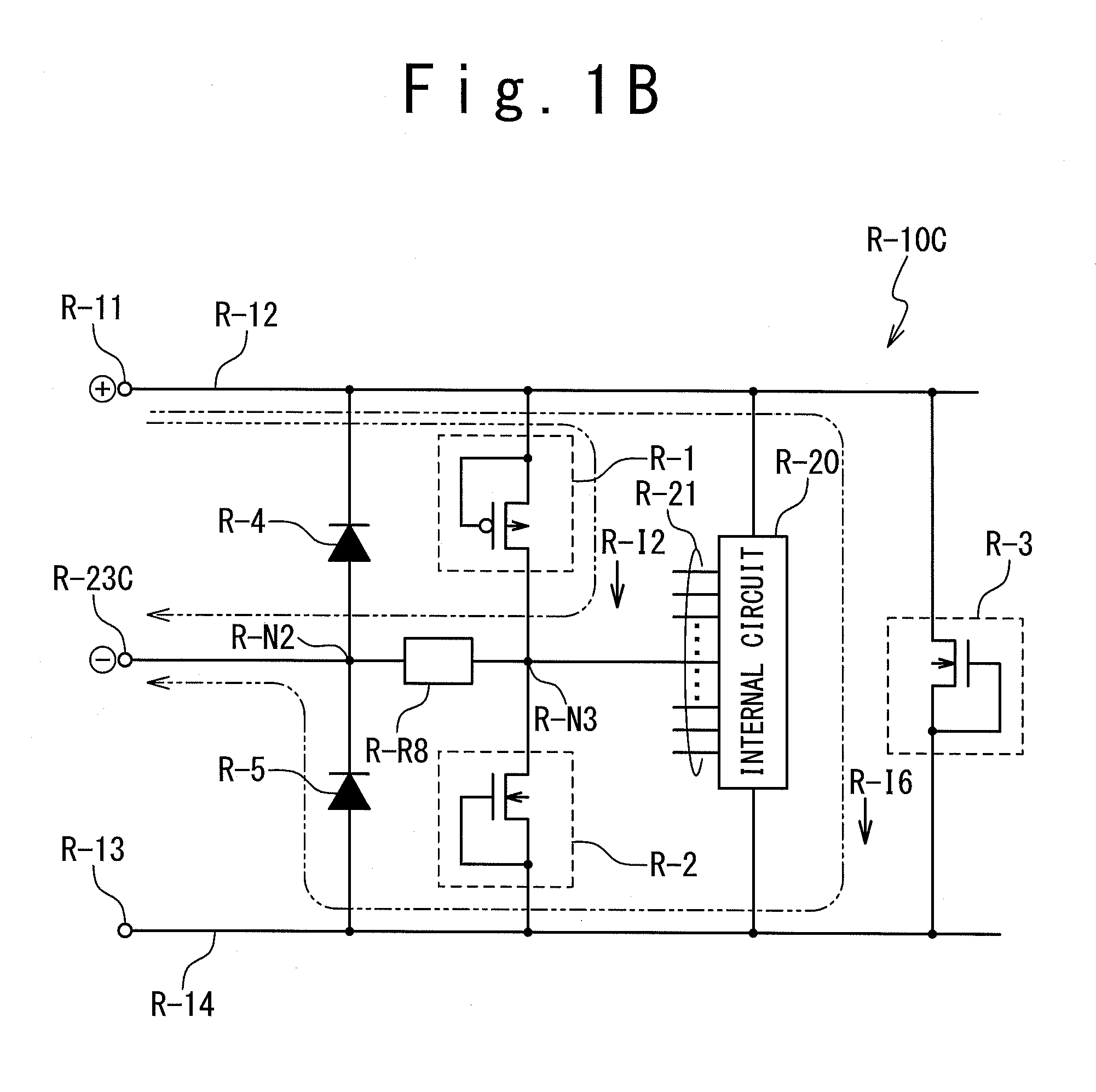
[0018]Hereinafter, some exemplary embodiments of the present invention will be described with reference to the drawings. FIG. 2 shows a configuration of a semiconductor device according to an embodiment of the present invention. The semiconductor device has an internal circuit 2 which is a semiconductor integrated circuit. The internal circuit 2 is operated by a power source system including a power source potential supplied from a power source potential line VDD connected to a power source terminal and a reference potential supplied from a ground potential line GND connected to a ground terminal. Further, the internal circuit 2 is connected to an input / output terminal I / O for inputting / outputting signals.

[0019]The semiconductor device has an electrostatic discharge protection circuit for protecting the internal circuit 2 from electrostatic discharge. The electrostatic discharge protection circuit includes a trigger circuit 12, a primary protection circuit 4, a resistor element 6, a...


PUM


Abstract

For enhancing performance of the electrostatic discharge protection for a semiconductor IC (integrated circuit), the electrostatic discharge protection circuit includes: a power source system for supplying a current to a semiconductor IC in the semiconductor device through a power source potential line and a reference potential line; a primary protection circuit for releasing a surge current to the power source system through a first node connected to a signal terminal when the surge current is generated at the signal terminal; a trigger circuit for generating a trigger signal in response to a surge voltage generated at the power source system; and a secondary protection circuit. The secondary protection circuit releases the surge current to the power source system through a second node connected between the first node and the semiconductor IC in response to the trigger signal, so that the surge voltage can be rapidly suppressed near the semiconductor IC.

Description

INCORPORATION BY REFERENCE[0001]This patent application is based on Japanese Patent Application No. 2009-137586. The disclosure of the Japanese Patent Application is incorporated herein by reference.BACKGROUND OF THE INVENTION[0002]1. Field of the Invention[0003]The present invention relates to a technique for protecting a semiconductor device from electrostatic discharge.[0004]2. Description of Related Art[0005]In recent years, mostly, semiconductor devices have electrostatic discharge protection circuits for protecting internal circuits from an electrostatic discharge (ESD) stress. In particular, since smaller and high speed operation circuits are desired, as a gate insulating-film of a field effect transistor (FET), a thinner insulating-film tends to be adopted. However, there is a problem that the tolerance of a thin gate insulating-film against electrostatic charges is low. Under the circumstances, more advanced protection means for electrostatic discharge is desired.[0006]As a...

Claims


Application Information

Patent Timeline
Patent Type & Authority Applications(United States)
IPC IPC(8): H02H9/04
CPCH02H9/046
Inventor MORISHITA, YASUYUKI
Owner RENESAS ELECTRONICS CORP
Why Eureka
Try Eureka