ER Doped III-Nitride Materials And Devices Synthesized by MOCVD

a technology of iiinitride and materials, which is applied in the direction of instruments, semiconductor lasers, optical elements, etc., can solve the problems of limiting the prospects of practical device applications in telecommunication systems

Active Publication Date: 2010-12-23
JIANG HONGXING +3
View PDF5 Cites 35 Cited by
  • Summary
  • Abstract
  • Description
  • Claims
  • Application Information

AI Technical Summary

Problems solved by technology

But all such devices still suffer either from strong emission lines in the visible region and / or from a low quantum efficiency at the IR wavelengths, severely limiting their prospects for practical device applications in telecommunication systems.

Method used


Image

  • ER Doped III-Nitride Materials And Devices Synthesized by MOCVD
  • ER Doped III-Nitride Materials And Devices Synthesized by MOCVD
  • ER Doped III-Nitride Materials And Devices Synthesized by MOCVD

Examples


Embodiment Construction

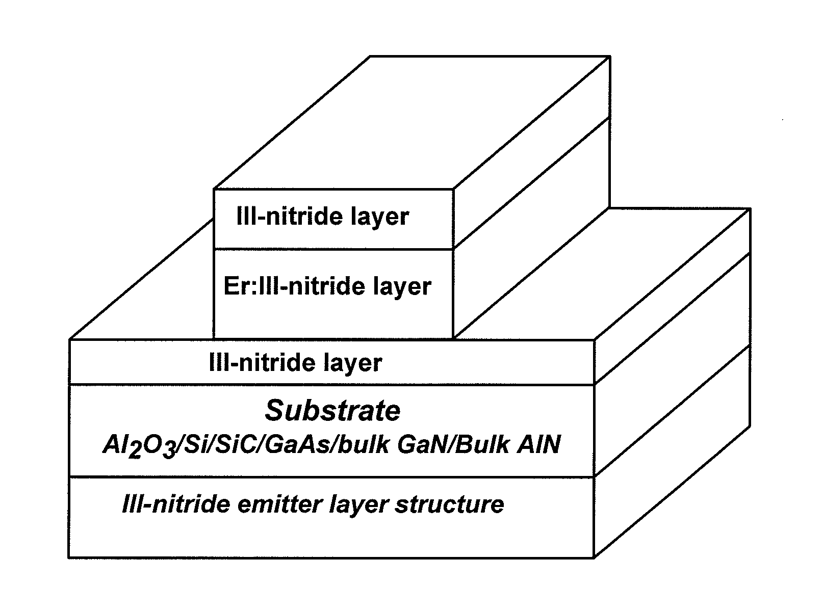
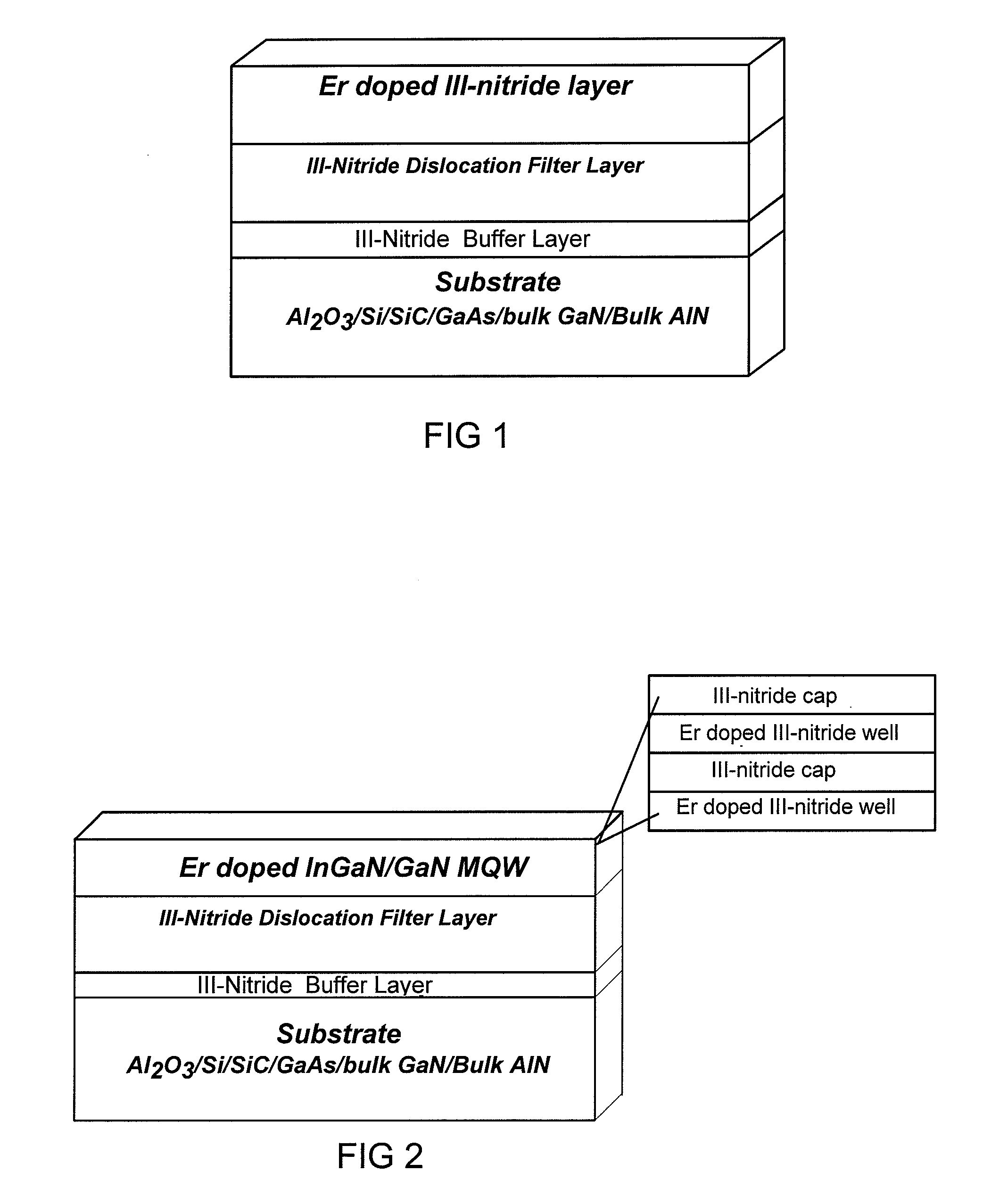
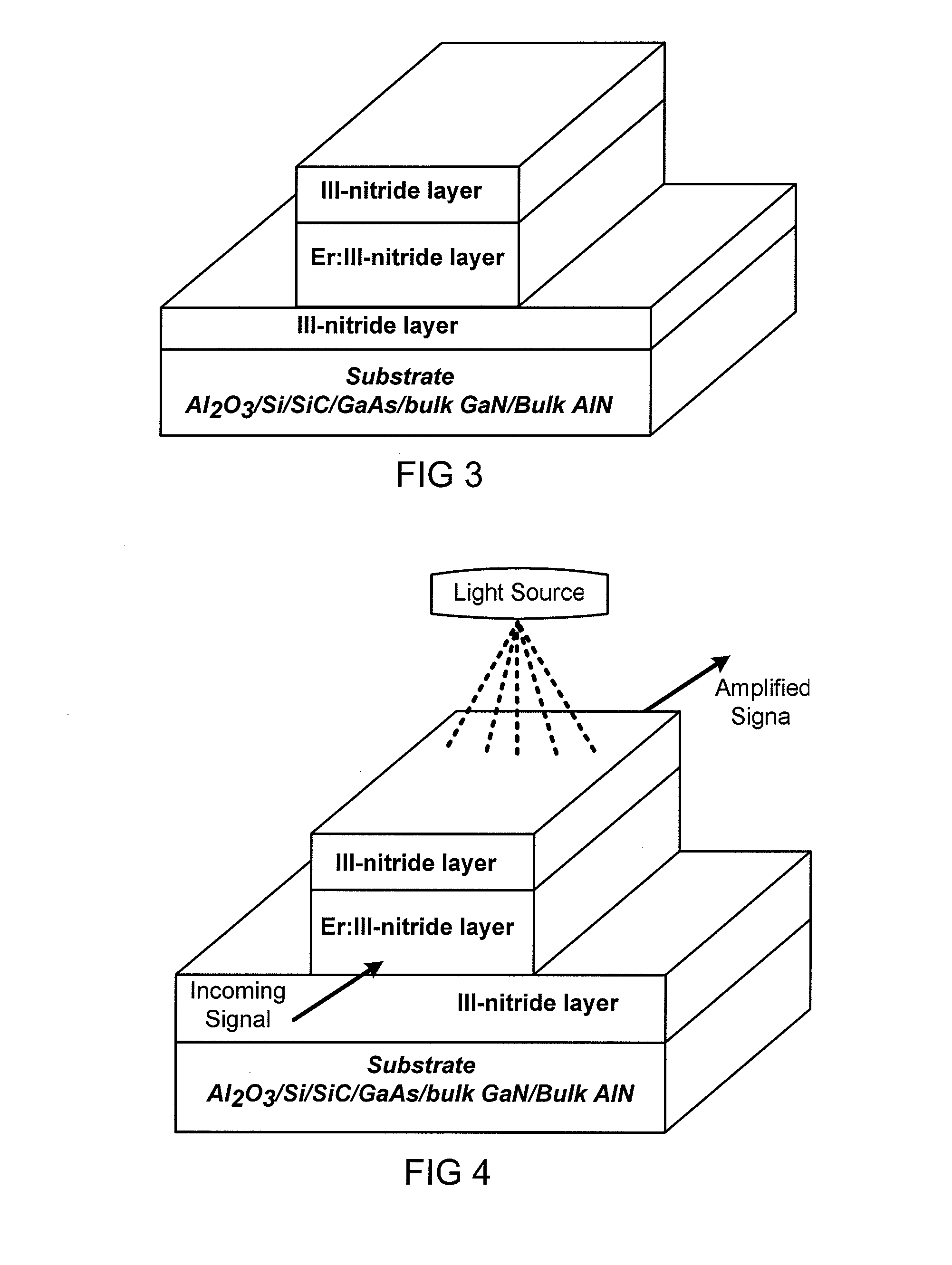
[0016]This disclosure relates to the synthesis of Er doped GaN epilayers by in-situ doping by metal-organic chemical vapor deposition (MOCVD). The optical and electrical properties of the Er doped GaN epilayers were studied by photoluminescence (PL) spectroscopy and Van der Pauw Hall method. Both above and below bandgap excitation results in a sharp PL emission peak at 1.54 μm. In contrary with other growth methods, MOCVD grown Er-doped GaN epilayers exhibit virtually no visible emission lines. A small thermal quenching effect, with only a 20% decrease in the integrated intensity of the 1.54 μm PL emission, occurred between 10 and 300 K. It was found that Er incorporation has very little effect on the electrical conductivity of the GaN epilayers and Er doped layers retain similar electrical properties as those of undoped GaN.

[0017]Er doped GaN obtained by in-situ incorporation by metal-organic chemical vapor deposition (MOCVD) has not been experimentally realized, even though device...


PUM

PropertyMeasurementUnit
wavelengthaaaaaaaaaa
emission wavelengthaaaaaaaaaa
excitation wavelengthaaaaaaaaaa

Abstract

This disclosure relates to the synthesis of Er doped GaN epilayers by in-situ doping by metal-organic chemical vapor deposition (MOCVD). In an embodiment, both above and below bandgap excitation results in a sharp PL emission peak at 1.54 μm. Contrary with other growth methods, MOCVD grown Er-doped GaN epilayers exhibit virtually no visible emission lines, an present a small thermal quenching effect. The Er incorporation has very little effect on the electrical conductivity of the GaN epilayers and Er doped layers retain similar electrical properties as those of undoped GaN.

Description

RELATED APPLICATIONS[0001]This application claims the benefit of U.S. Provisional Patent Application No. 60 / 823,465 filed Aug. 24, 2006.BACKGROUND OF THE INVENTION[0002]Incorporation of rare-earth atoms into a semiconductor host has received much attention recently due to the potential applications of rare-earth doped materials as efficient optical amplifiers and light-emitters. The outer 5s and 5p shells shield the inner 4f electrons from the surrounding environment, allowing the energy levels of the 4f shell to remain relatively unperturbed when placed into a solid host. By choosing the appropriate rare-earth element, it is possible to create very sharp, temperature-stable light emission based upon intra-4f transitions. A majority of the research done for rare-earth doping has been devoted to the element Er, since one of its 4f transitions produces emission at wavelength (1.54 μm) that corresponds to a minimum loss in modern silica fibers for optical communications. Much of the ea...

Claims


Application Information

Patent Timeline
Patent Type & Authority Applications(United States)
IPC IPC(8): H01L33/00H01L21/443H01L33/30
CPCB82Y20/00H01S5/32341H01L21/0237H01L21/02458H01L21/0254H01L21/02581H01L27/15H01L29/2003H01L29/207H01L33/305H01S3/0632H01S3/0637H01S3/0933H01S3/0941H01S3/09415H01S3/1608H01S3/1628H01S3/2383H01S5/026H01S5/183G02B6/1225
Inventor JIANG, HONGXINGLIN, JINGYUUGOLINI, CRISZAVADA, JOHN
Owner JIANG HONGXING
Why Eureka
Try Eureka