Near-field light generating device that includes near-field light generating element accommodated in a groove of an encasing layer
- Summary
- Abstract
- Description
- Claims
- Application Information
AI Technical Summary
Benefits of technology
Problems solved by technology
Method used
Image


Examples
first embodiment
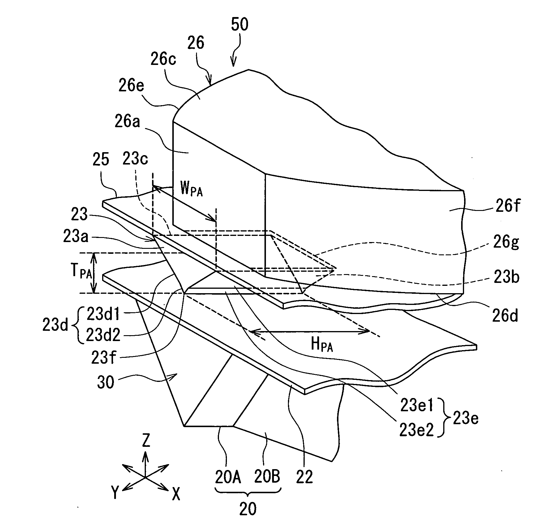
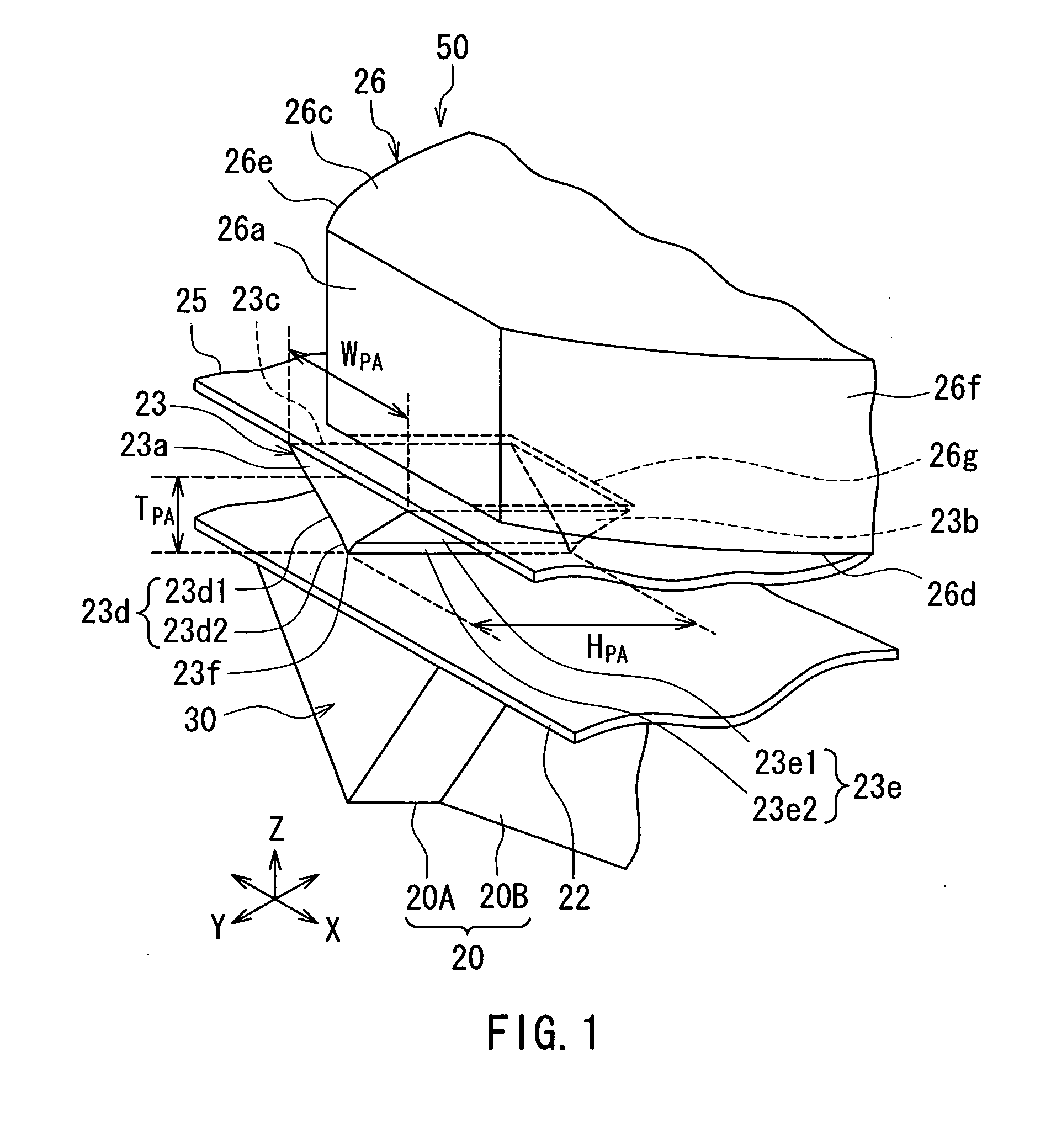
[0060]Preferred embodiments of the present invention will now be described in detail with reference to the drawings. Reference is first made to FIG. 7 to describe a magnetic disk drive and a slider including a heat-assisted magnetic recording head according to a first embodiment of the invention. FIG. 7 is a perspective view of the slider including the heat-assisted magnetic recording head according to the present embodiment.
[0061]The magnetic disk drive of the present embodiment incorporates the slider 200 including the heat-assisted magnetic recording head according to the present embodiment. The slider 200 is supported by a suspension (not shown) and is disposed to face a circular-plate-shaped recording medium (magnetic disk) that is driven to rotate. In FIG. 7 the X direction is a direction across the tracks of the recording medium, the Y direction is a direction perpendicular to the surface of the recording medium, and the Z direction is the direction of travel of the recording...
modification example
[0139]A modification example of the present embodiment will be now described. FIG. 24 is a perspective view showing the near-field light generating element 23 and its vicinity in a heat-assisted magnetic recording head according to the modification example of the present embodiment. In this modification example, the near-field light generating element 23 has a groove 23g that opens in the top surface 23c. The groove 23g is V-shaped in a cross section parallel to the medium facing surface 30. Accordingly, the first and second end faces 23a and 23b of the near-field light generating element 23 are generally V-shaped. The heat-assisted magnetic recording head of the modification example further has a dielectric layer 51 disposed in the groove 23g. The dielectric layer 51 is made of the same material as that of the waveguide 26, for example. The near-field light generating element 23, the dielectric layer 51 and the encasing layer 24 are flattened at the top. The interposition layer 25 ...
second embodiment
[0141]A second embodiment of the present invention will now be described with reference to FIG. 25. FIG. 25 is a perspective view of the near-field light generating element according to the present embodiment. The near-field light generating element 23 according to the present embodiment is configured so that an area near the first end face 23a (hereinafter, referred to as front end vicinity area) has a bottom end that gets farther from the top surface 1a of the substrate 1 with decreasing distance to the first end face 23a. Only in the front end vicinity area of the near-field light generating element 23, each of the side surfaces 23d and 23e includes an upper part and a lower part that are continuous with each other, and the angle formed between the lower part of the side surface 23d and the lower part of the side surface 23e is smaller than that formed between the upper part of the side surface 23d and the upper part of the side surface 23e. In the area other than the front end v...
PUM
 Abstract
Description
Claims
Application Information
PatSnap Eureka turns technology decisions into work you can execute. Powered by our Innovation Knowledge Graph, it runs expert workflows across engineering, life sciences, materials and intellectual property. Get your review-ready output in minutes.


