Light emitting device and method for manufacturing same
a technology of light emitting devices and manufacturing methods, applied in semiconductor/solid-state device manufacturing, semiconductor devices, electrical equipment, etc., can solve the problems of low long-term reliability, difficult manufacturing of zd, and large burden, and achieve the effect of suppressing optical shielding and optical absorption, reducing optical output, and preferable luminance withou
- Summary
- Abstract
- Description
- Claims
- Application Information
AI Technical Summary
Benefits of technology
Problems solved by technology
Method used
Image
Examples
embodiment 1
[0093]One embodiment of the present invention is described below with reference to drawings.
(Arrangement of Light Emitting Device)
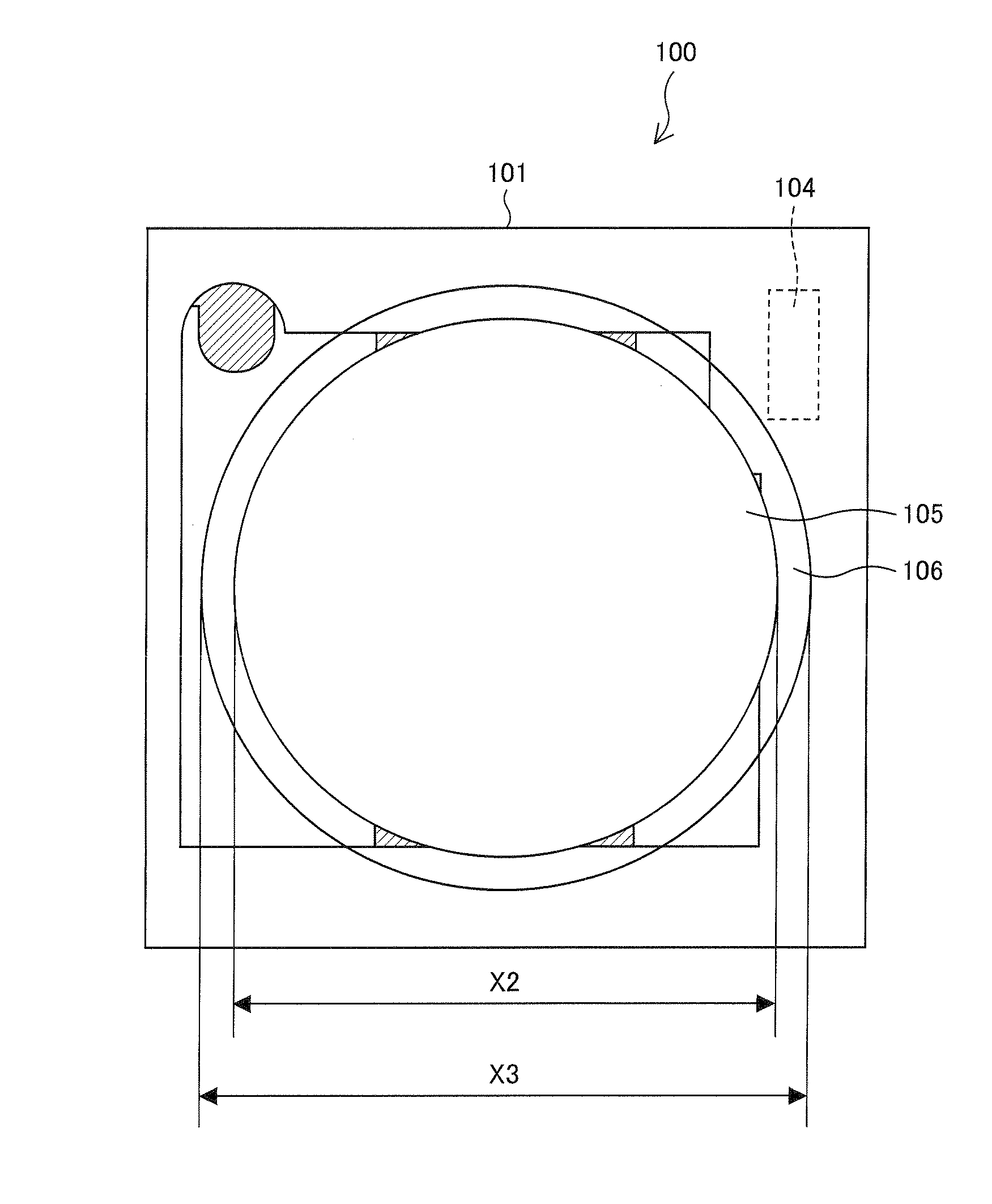
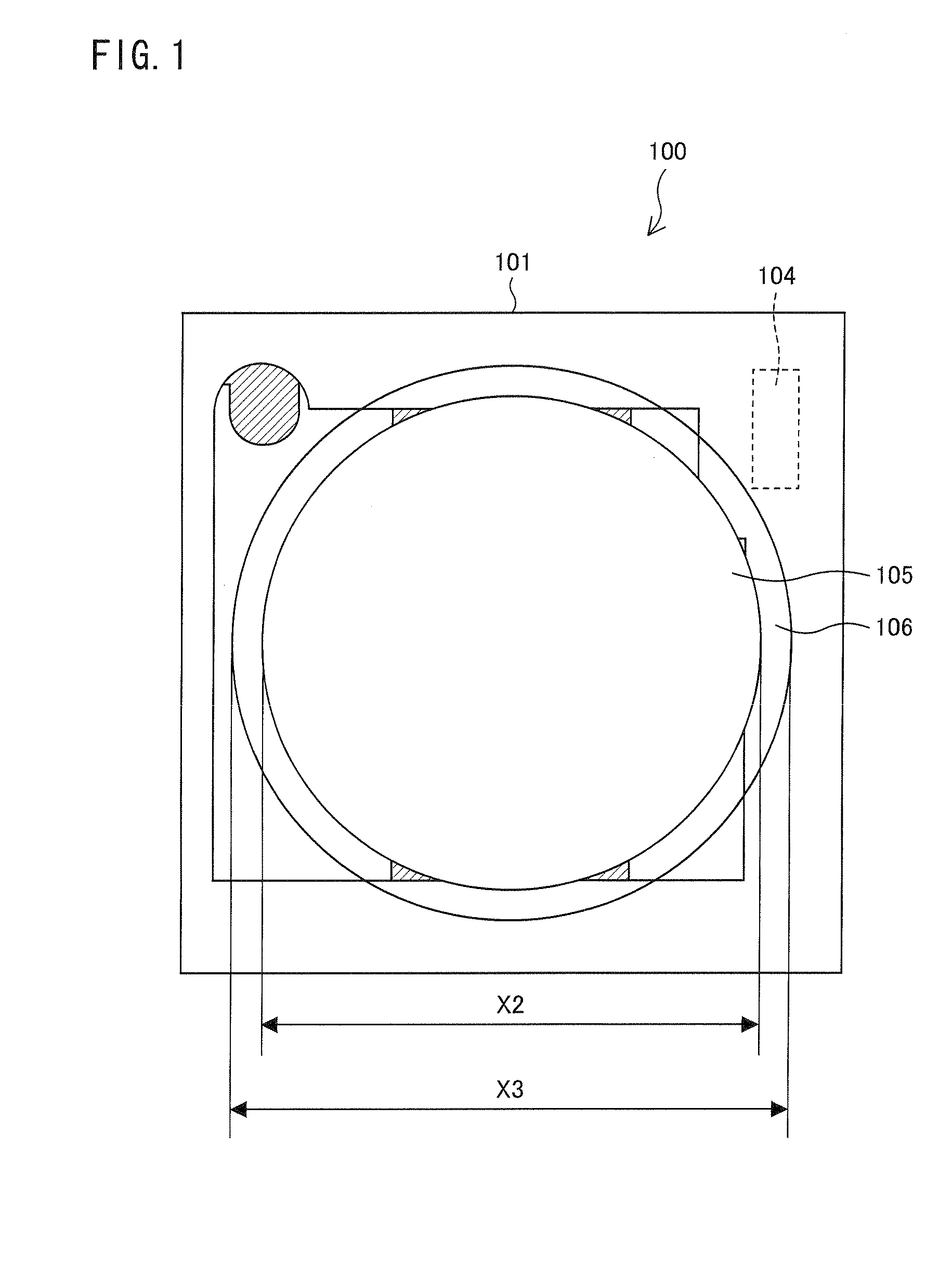
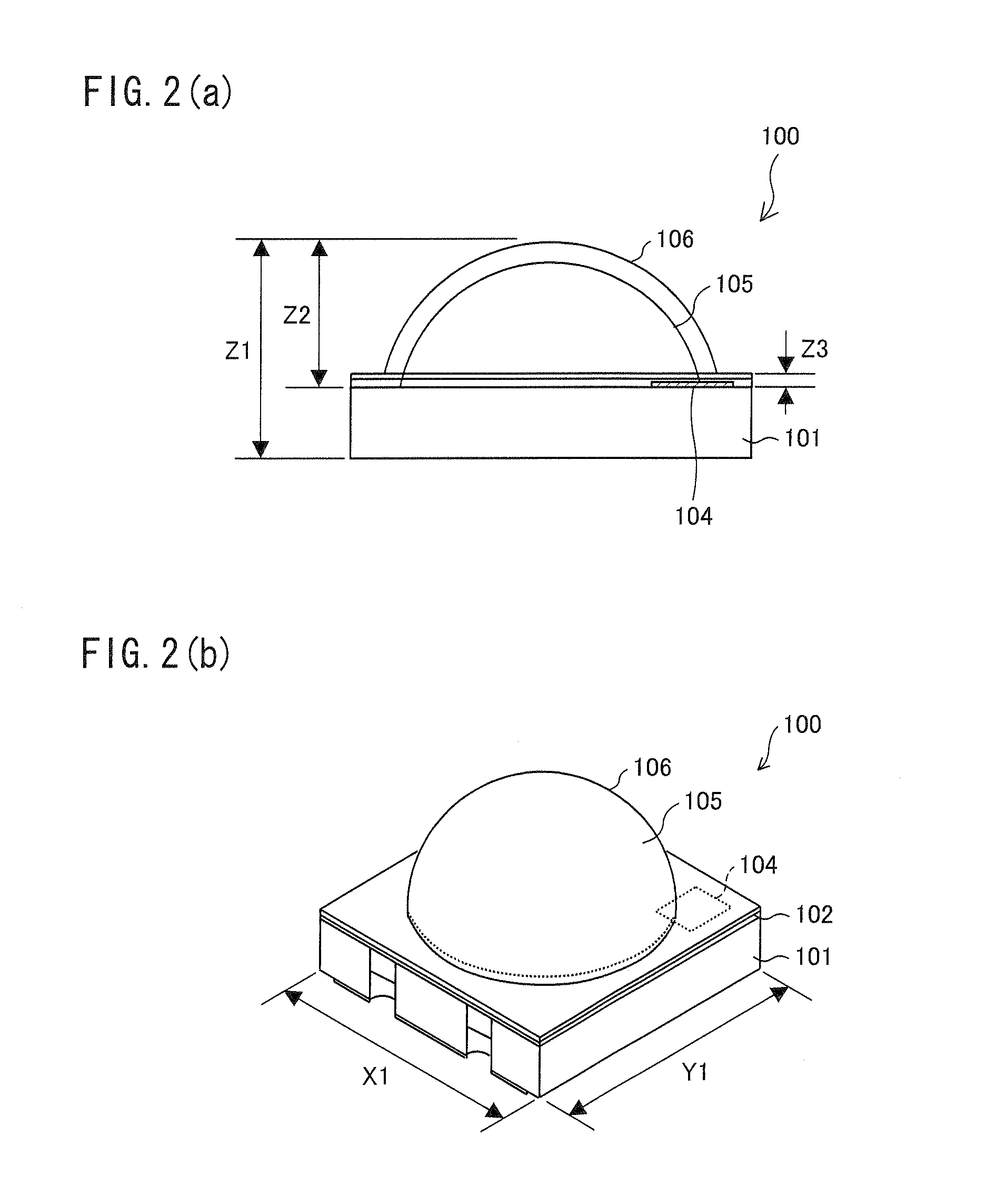
[0094]FIG. 1 is a top view illustrating an example of an arrangement of a light emitting device 100 of the present embodiment. FIG. 2(a) is a side view illustrating the light emitting device 100 illustrated in FIG. 1. FIG. 2(b) is a perspective view illustrating the light emitting device 100 illustrated in FIG. 1. FIG. 3 is a perspective view obtained in a case where the light emitting device 100 of FIG. 1 is viewed from above.
[0095]The light emitting device 100 includes: a substrate 101; a glass layer 102; LED chips 103 (semiconductor light emitting elements); a printed resistor element 104; a fluorescent material-containing resin layer 105; and a transmissive resin layer 106 (see FIGS. 1 through 3).
[0096]The substrate 101 is a ceramic substrate made from ceramics. The glass layer 102, the LED chips 103, the printed resistor element 104, the fluorescent ...
embodiment 2
[0163]According to the light emitting device 100 of Embodiment 1, the plurality of LED chips are doubly sealed with the fluorescent material-containing resin layer 105 and the transmissive resin layer 106. However, the present invention is not limited to this, and the plurality of LED chips can be sealed with at least one of the fluorescent material-containing resin layer 105 and the transmissive resin layer 106. That is, the sealing resin can be selected in accordance with a sort of LED chip 103 and / or a design of an emission color.
[0164]FIG. 13(a) is a cross-sectional view illustrating an example of an arrangement of a light emitting device 200 of the present embodiment. FIG. 13(b) is a perspective view obtained in a case where the light emitting device 200 is viewed from above. The light emitting device 200 has an arrangement in which no transmissive resin layer 106 is provided in the light emitting device 100 of Embodiment 1 (see FIGS. 13(a) and 13(b)).
[0165]In the light emittin...
embodiment 3
[0167]According to the light emitting device 100 of Embodiment 1, each of the fluorescent material-containing resin layer 105 and the transmissive resin layer 106 has a dome shape. However, the present invention is not limited to this, provided that each of the fluorescent material-containing resin layer 105 and the transmissive resin layer 106 has a shape which allows the light emitted from the plurality of LED chips 103 to uniformly outgo to the outside from the entire surface on which LED chips 103 are provided.
[0168]FIG. 14(a) is a cross-sectional view illustrating an example of an arrangement of a light emitting device 300 of the present embodiment. FIG. 14(b) is a perspective view obtained in a case where the light emitting device 300 is viewed from above. The light emitting device 300 has an arrangement similar to that of the light emitting device 100 of Embodiment 1, except for a shape of the fluorescent material-containing resin layer 105 (see FIGS. 14(a) and 14(b)).
[0169]A...
PUM
 Abstract
Description
Claims
Application Information


