Push-pull programmable logic device cell

a technology of programmable logic and push-pull, which is applied in the direction of pulse technique, logic circuit, instruments, etc., can solve the problems of product employing such a cell, off device degradation, etc., and achieve the effect of reducing stress

Active Publication Date: 2011-01-06
MICROSEMI SOC
View PDF70 Cites 29 Cited by
  • Summary
  • Abstract
  • Description
  • Claims
  • Application Information

AI Technical Summary

Benefits of technology

[0010]According to one aspect of the present invention, stress may be reduced in one or both of the non-volatile transistors in a push-pull memory cell by providing at least one stress transistor in the memory cell. In the illustrative embodiments disclosed herein, a stress transistor may be provided between either the non-volatile n-channel transistor and the switch transistor, the non-volatile p-channel transistor and the switch transistor, or between both the non-volatile n-channel transistor and the switch transistor and the non-volatile p-channel transistor and the switch transistor. In other illustrative embodiments, a stress transistor may be provided between either the non-volatile n-channel transistor and ground, or the non-volatile p-channel transistor and VDD.

Problems solved by technology

For many non-volatile memory devices this can cause the off device to degrade over time.
Prior art patents disclose full push-pull non-volatile memory cells, however it is not believed that there is an actual product employing such a cell has not been reported.

Method used


Image

  • Push-pull programmable logic device cell
  • Push-pull programmable logic device cell
  • Push-pull programmable logic device cell

Examples


Embodiment Construction

[0019]Persons of ordinary skill in the art will realize that the following description of the present invention is illustrative only and not in any way limiting. Other embodiments of the invention will readily suggest themselves to such skilled persons.

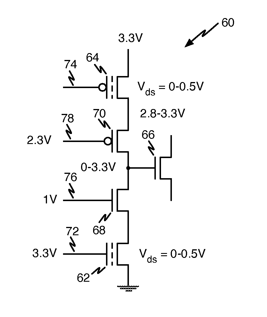
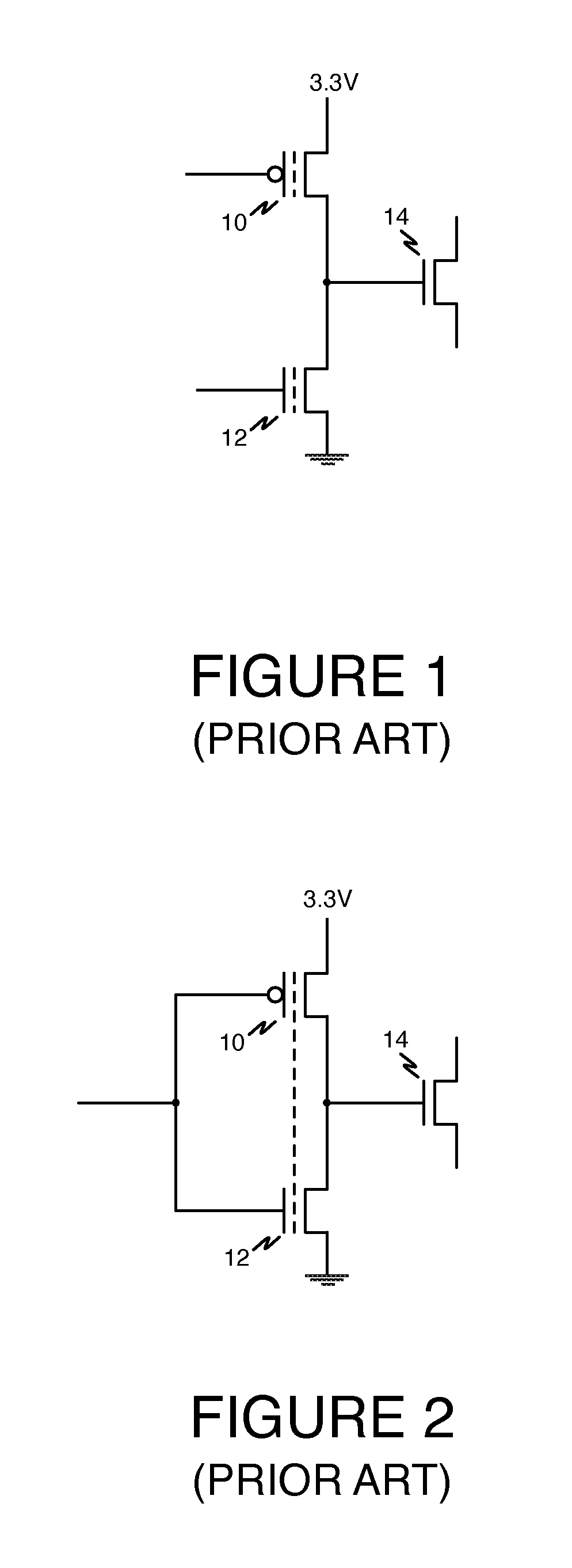
[0020]The problem encountered in prior-art non-volatile push-pull memory cells can be alleviated by placing at least one additional transistor in the cell order to limit the Vds of the non-volatile p-channel transistor, the non-volatile n-channel transistor, or both to around 0.5V and still allow the output to the gate of the switch transistor to be either at least a full 2.5V or even higher to fully turn on the switch transistor or at ground to fully turn off the switch transistor. In some embodiments, stress is relieved to the non-volatile p-channel transistor, the non-volatile n-channel transistor, or both.

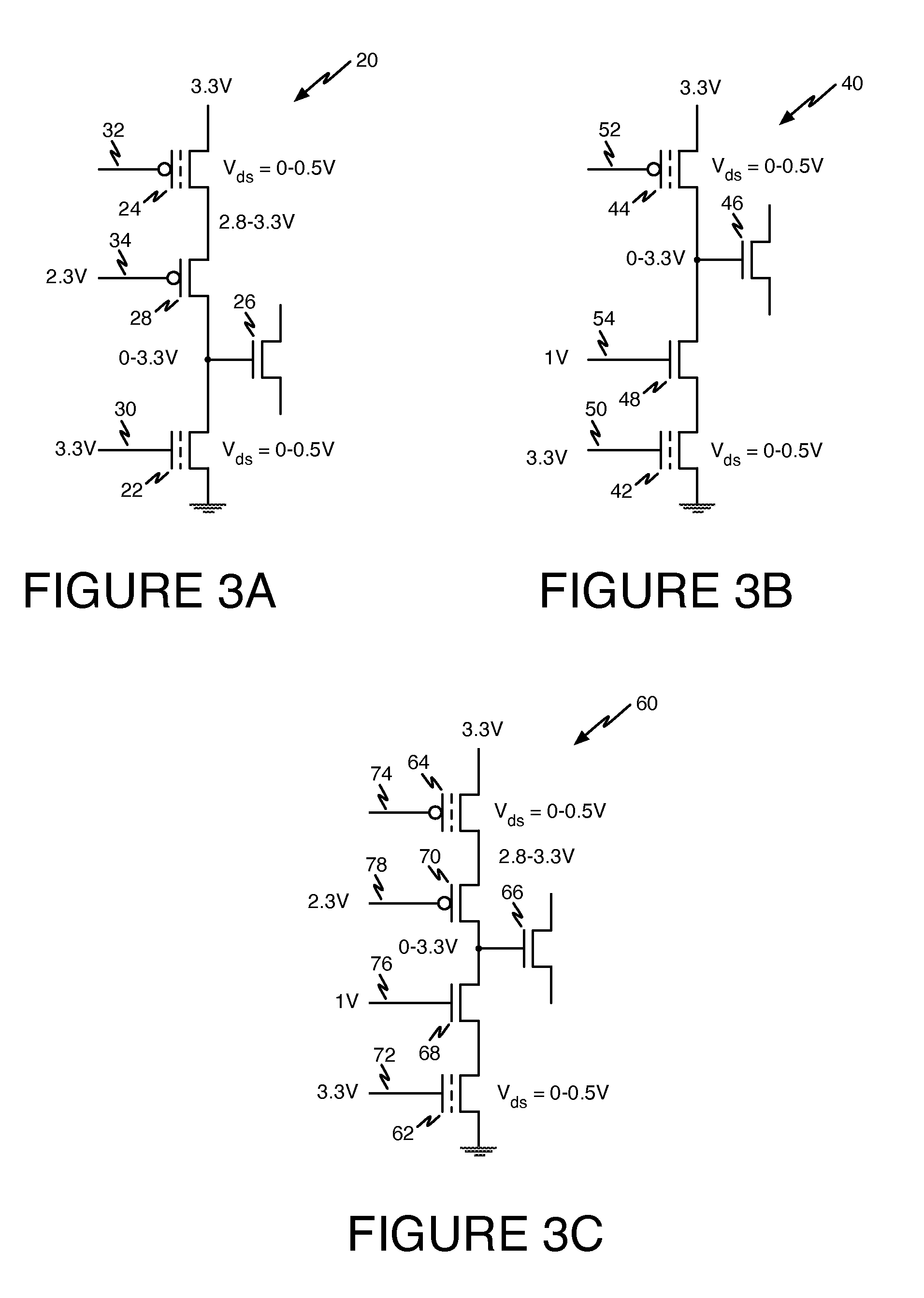
[0021]Referring now to FIG. 3A, a schematic diagram shows an illustrative push-pull non-volatile memory cell 20 in order to sho...


PUM


Abstract

A memory cell includes a non-volatile p-channel transistor having a source coupled to a first potential, a drain, and a gate. A non-volatile n-channel transistor has a source coupled to a second potential, a drain, and a gate. A switch transistor has a gate coupled to a switch node, a source, and a drain. A stress transistor has a source and drain coupled between the drain of the non-volatile p-channel transistor and the drain of the non-volatile n-channel transistor, the stress transistor having a gate coupled to a gate bias circuit. Where one of the first or second potentials is a bit line, an isolation transistor is coupled between the other of the second potentials and one of the non-volatile transistors.

Description

CLAIM FOR PRIORITY[0001]This application claims the benefit of U.S. Provisional Application Ser. No. 61 / 222,708, filed on Jul. 2, 2009, the entirety of which is incorporated by reference herein.BACKGROUND[0002]1. Field of the Invention[0003]The present invention relates to non-volatile memory cells in push-pull configuration. More particularly, the present invention relates to non-volatile memory cells in push-pull configuration that may be employed in FPGA devices.[0004]2. The Prior Art[0005]Push-pull non-volatile memory cells for FPGAs have been previously proposed, as shown by illustrative examples in FIGS. 1 and 2. As shown in both FIGS. 1 and 2, a basic push-pull non-volatile memory cell for use in an FPGA device includes a non-volatile p-channel memory transistor 10 connected in series with a non-volatile n-channel memory transistor 12. The common drain connections of the non-volatile p-channel memory transistor 10 and the non-volatile n-channel memory transistor 12 are connec...

Claims


Application Information

Patent Timeline
Patent Type & Authority Applications(United States)
IPC IPC(8): G11C16/04
CPCH01L27/2436H01L27/2463H01L45/085H01L45/1266H01L45/141H01L45/142H01L45/1253H01L45/1616H01L45/1625H01L45/1675H01L45/122H01L45/1233Y10S438/90H01L45/149H03K19/17724H03K19/1776G11C13/0011H10B63/30H10B63/80H10N70/245H10N70/826H10N70/8416H10N70/882H10N70/8822H10N70/8845H10N70/023H10N70/026H10N70/063H10N70/011H10N70/821H10N70/841H10N70/24
Inventor MCCOLLUM, JOHN
Owner MICROSEMI SOC
Why Eureka
Try Eureka