Composite electronic device

Active Publication Date: 2011-01-13
TDK CORPARATION
View PDF3 Cites 88 Cited by
  • Summary
  • Abstract
  • Description
  • Claims
  • Application Information

AI Technical Summary

Benefits of technology

[0025]The composite electronic device according to the present invention further includes a third ESD protection element connected to the other end of the first spiral conductor, and a fourth ESD protection element connected to the other end of the second spiral conductor. The third and fourth ESD protection elements have the same configurations as those of the first and second ESD protection elements. The gap protection layer is preferably provided on at least the upper side or the lower side of the third and fourth ESD protection element. According to this configuration, because the ESD protection elements are connected to both of a pair of input ends and a pair of output ends of the composite electronic device, the composite electronic device can be mounted without requiring consciousness of a direction of connection to a pair of signal lines. Consequently, handl

Problems solved by technology

However, this circuit generates a relatively large radiation electromagnetic field when common noise (common mode noise) is superimposed on the signal lines 1 and 2.
Accordingly, ESD (electrostatic discharge) becomes a large problem.
However, when the varistor is used, a signal waveform becomes inert, and signal quality is degraded.
Therefore, the ESD prot

Method used


Image

  • Composite electronic device
  • Composite electronic device
  • Composite electronic device

Examples


example

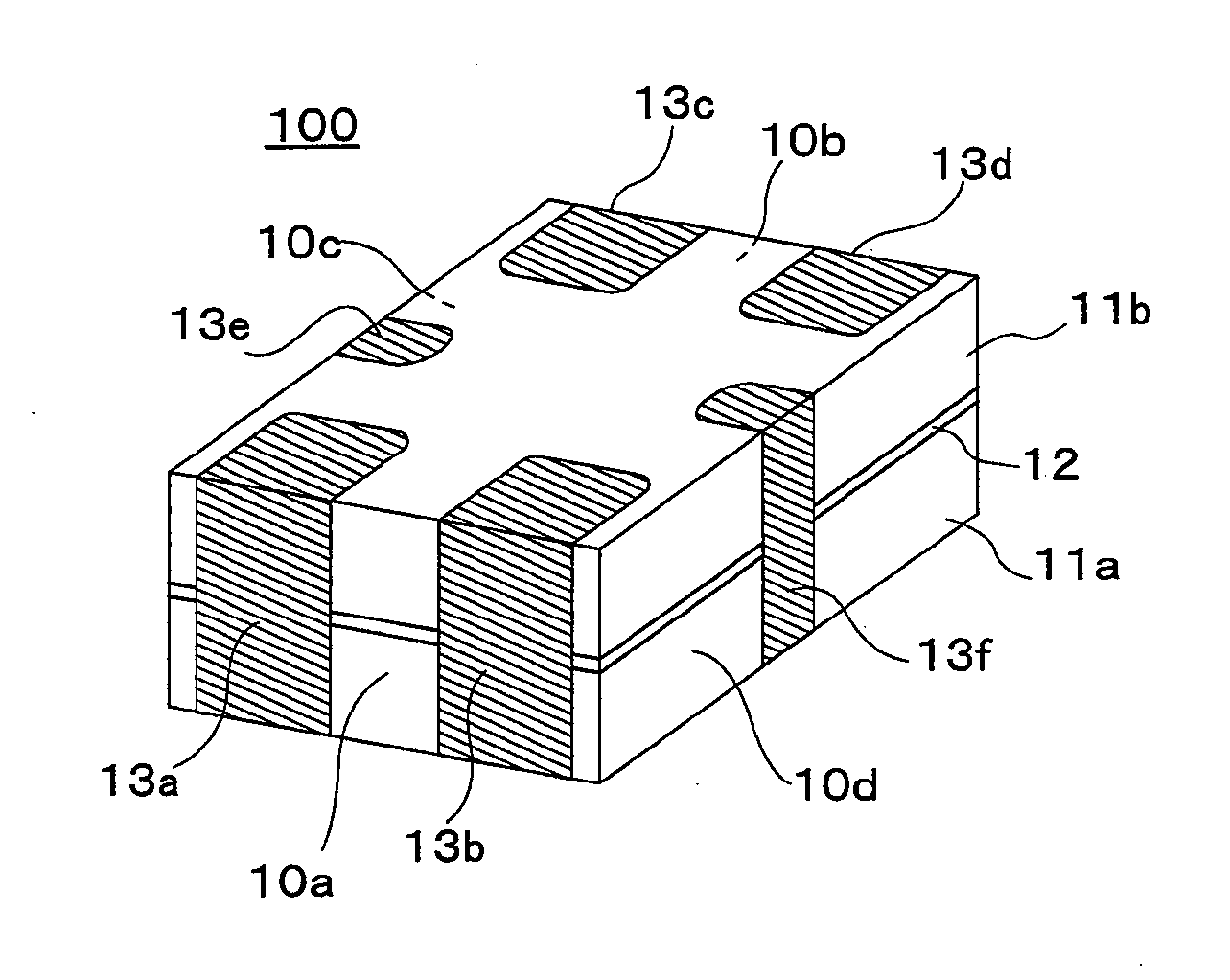
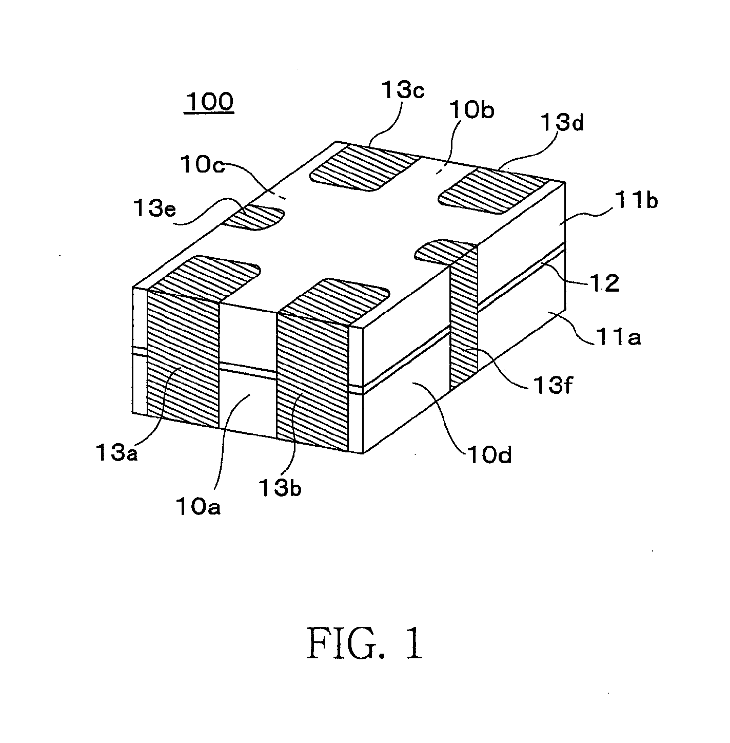
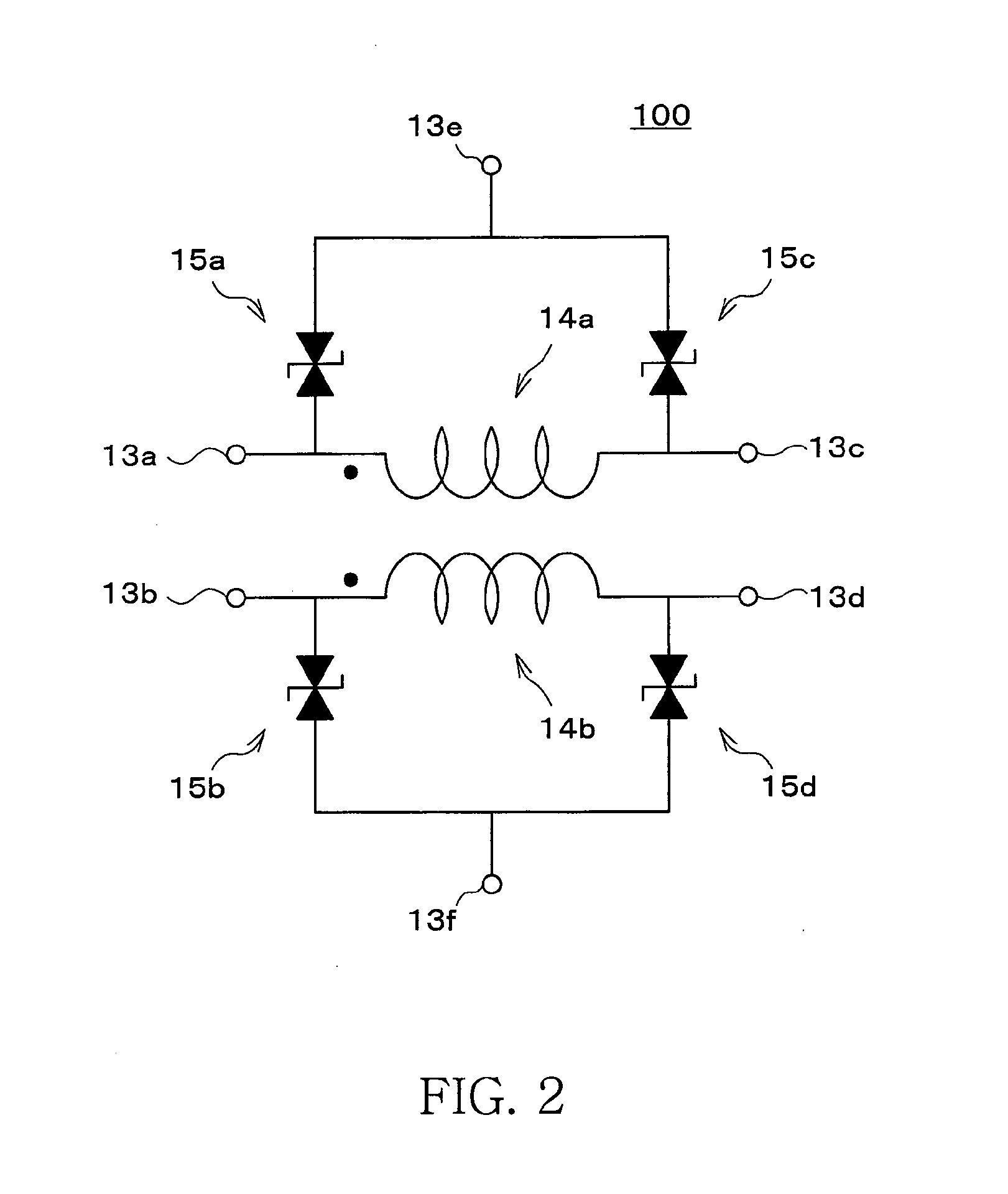
[0124]A sample of a composite electronic device according to the example that is configured by combining the common mode filter element and the ESD protection element having the gap protection layer made of composite ferrite containing carbon is prepared. As shown in FIG. 10, this sample includes magnetic substrates 11a and 11b made of sintered ferrite, an insulation layer 27 that is formed on the magnetic substrate 11a, is made of Al2O3, and has the thickness of about 3 μm, an ESD absorbing layer 33 formed on the insulation layer 27, and a gap protection layer 16g that is formed on the ESD absorbing layer 33 and is made of composite ferrite containing carbon. The ESD absorbing layer 33 includes gap electrodes 28 to 31 that are formed on the insulation layer made of Al2O3 and are made of a Cr / Cu film having the thickness of about 4000 Å, a conductive inorganic material 35 that is formed on the gap electrodes 28 to and is made of Au, and an insulation inorganic material 34 that is pr...


PUM


Abstract

The present invention is provided with a composite electronic device comprising an inductor element and an ESD protection element formed between two magnetic substrates, wherein the inductor element includes insulation layers made of a resin, and spiral conductors formed on the insulation layers, the ESD protection element includes a base insulation layer, a pair of gap electrodes arranged via gap formed therebetween on the base insulation layer, and an ESD absorbing layer arranged at least between the gap electrodes, and a gap protection layer provided on at least one of the upper side and lower side of the gap, the ESD absorbing layer includes a composite material having an insulation inorganic material and a conductive inorganic material discontinuously dispersed in a matrix of the insulation inorganic material. The gap protection layer is made of resin including magnetic powder and carbon.

Description

TECHNICAL FIELD[0001]The present invention relates to a composite electronic device, and, more particularly relates to a structure of a composite electronic device constituted by combining inductor elements and electrostatic discharge (ESD) protection elements.BACKGROUND OF THE INVENTION[0002]In recent years, standards of USB 2.0 and a high-definition multimedia interface (HDMI) have been widely distributed as high-speed signal transmission interfaces, and they are used in many digital devices such as personal computers and digital high-vision televisions. These interfaces employ a differential signal system that transmits a differential signal (a differential mode signal) by using a pair of signal lines, unlike a single-end transmission system that has been generally used for many years.[0003]The differential transmission system has excellent characteristics in that the system is not easily affected by exogenous noise as well as that the system has a small radiation electromagnetic...

Claims


Application Information

Patent Timeline
IPC IPC(8): H02H9/00H02H3/22
CPCH01F17/0006H01F19/00H03H7/427H03H2001/0085H03H7/0107
Inventor ASAKAWA, MASAOITO, TOMOKAZUMORITA, MAKOTOHITOMI, ATSUSHIHIROBE, YASUHIROASAKURA, KENSAKU
Owner TDK CORPARATION
Why Eureka
Try Eureka