NAND type ROM

a technology of nand type and rom, applied in the field of nand type rom, can solve the problems of erroneous read data, more significant crosstalk, low operating speed and read errors, etc., and achieve the effect of reducing read errors and increasing reading speed

Inactive Publication Date: 2011-01-13
NATIONAL TSING HUA UNIVERSITY
View PDF2 Cites 9 Cited by
  • Summary
  • Abstract
  • Description
  • Claims
  • Application Information

AI Technical Summary

Benefits of technology

As stated above, the present invention may provide one or more of the following advantages:
(2) The NAND type ROM allows no voltage drop caused by capacitance coupling to occur between the adjacent bit lines and the reduction of read errors such that the NAND type ROM has full code-coverage and an increased reading speed.

Problems solved by technology

In designing read-only memories (ROMs), code-dependent crosstalk leads to problems such as lower operating speeds and read errors.
Due to a coupling noise arisen by the parasitic capacitances of the adjacent bit lines BL[0] and BL[2], the voltage of the transistor 412 on the bit line BL[1] should be a constant value but the voltage drop results the erroneous read data.
Furthermore, a greater voltage swing at the bit lines causes a more significant crosstalk.

Method used


Image

  • NAND type ROM
  • NAND type ROM
  • NAND type ROM

Examples


Embodiment Construction

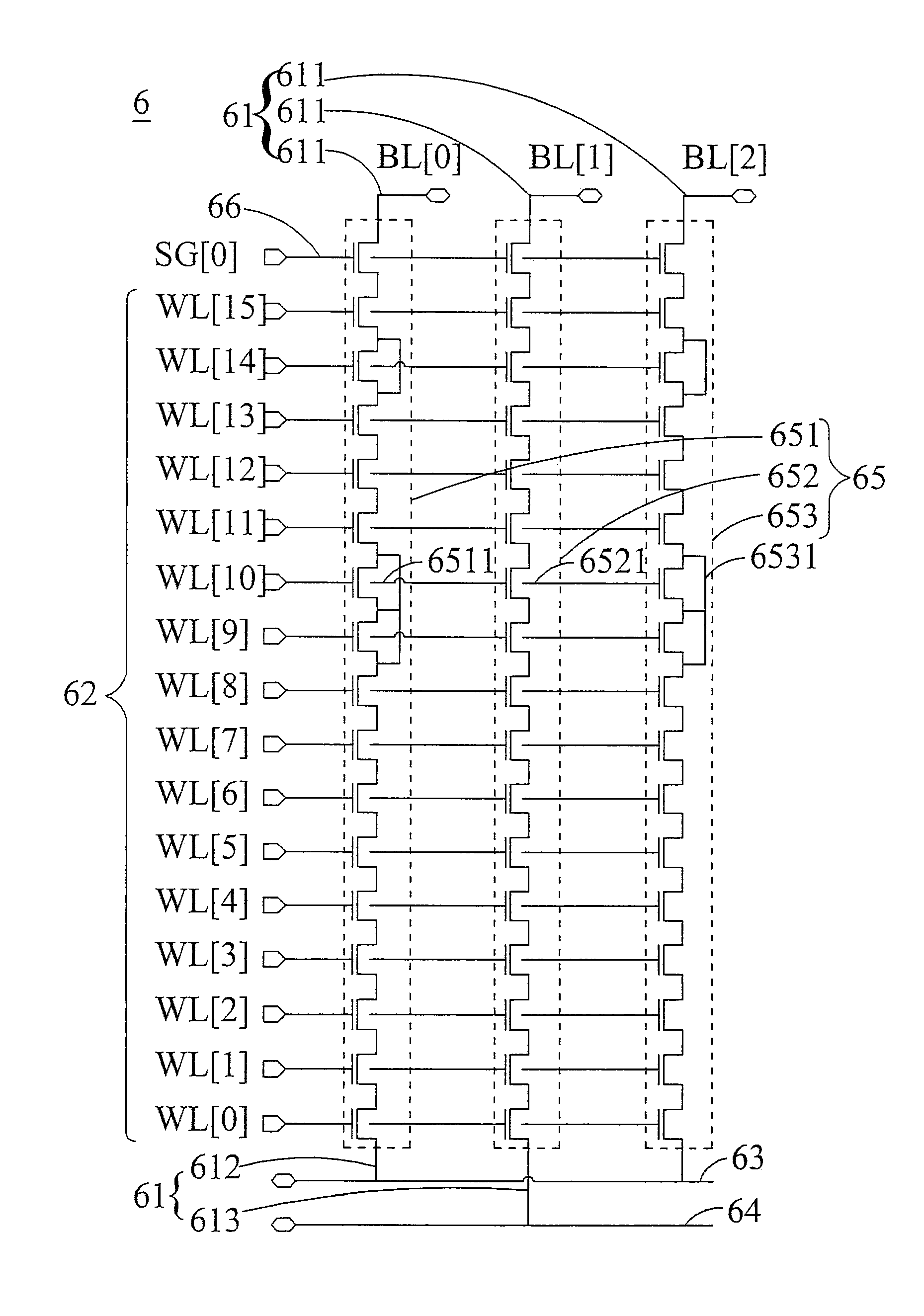
Referring to FIG. 6, in which a schematic view of a NAND type ROM of the present invention is shown. The NAND type ROM 6 comprises a plurality of bit lines 61, a plurality of word lines 62, a first source line 63, a second source line 64, and a plurality of NAND strings 65. The plurality of bit lines 61 comprise a plurality of upper bit lines 611, a plurality of first lower bit lines 612, and a plurality of second lower bit lines 613. The plurality of first lower bit lines 612 and the plurality of second lower bit lines 613 are alternately arranged in parallel, and the plurality of word lines 62 are vertically arranged to each bit lines 61. The first source line 63 is connected to the plurality of first lower bit lines 62. The second source line 64 is connected to the plurality of second lower bit lines 613. The plurality of NAND strings 65 comprise a plurality of first NAND strings 651 and a plurality of second NAND strings 652. The plurality of first NAND strings 651 are connected...


PUM


Abstract

The invention discloses a NAND type ROM. The NAND type ROM comprises a plurality of bit lines, a plurality of word lines, a first source line, a second source line, and a plurality of NAND strings. The bit lines comprise a plurality of upper bit lines, first lower and second lower bit lines. The first lower and second lower bit lines are alternately arranged in parallel, and the plurality of word lines are vertically arranged to each bit lines. The first and second source line are respectively connected to the plurality of first and second lower bit lines. The plurality of NAND strings comprise a plurality of first and second NAND strings. The first NAND strings are connected to the upper bit lines, word lines, and first lower bit lines. The second NAND strings are connected to the upper bit lines, word lines, and second lower bit lines.

Description

BACKGROUND OF THE INVENTION(a) Field of the InventionThe present invention relates a NAND type ROM, and more particularly to a NAND type ROM that solves a crosstalk problem by a first source line and a second source line which are alternately arranged.(b) Description of the Prior ArtIn designing read-only memories (ROMs), code-dependent crosstalk leads to problems such as lower operating speeds and read errors. Such crosstalk is caused because bit lines are adjacently disposed and thus the parasitic capacitances effect occurs between every two adjacent bit lines. As illustrated in FIG. 1, in which a schematic view of a NAND type ROM array of the prior art is illustrated. In this figure, the ROM array comprises a plurality of NAND strings 11 and a plurality of bit lines (BL) 12. The bit lines 12 are adjacently disposed, so the parasitic capacitances 13 are arisen between every two adjacent bit lines.Referring to FIG. 2, in which a schematic view of a NAND string of the prior art is s...

Claims


Application Information

Patent Timeline
Patent Type & Authority Applications(United States)
IPC IPC(8): G11C16/04
CPCG11C17/18G11C17/16
Inventor CHANG, MENG-FANLIANG, CHIH-WEICHIANG, CHIH-CHYUANG
Owner NATIONAL TSING HUA UNIVERSITY
Why Eureka
Try Eureka