

Power semiconductor module and method of manufacturing the same
- Summary
- Abstract
- Description
- Claims
- Application Information
AI Technical Summary
Benefits of technology
Problems solved by technology
Method used
Image

Examples
Embodiment Construction
[0038]Various objects, advantages and features of the invention will become apparent from the following description of embodiments with reference to the accompanying drawings. Throughout the accompanying drawings, the same reference numerals are used to designate the same or similar components. For the clarity of description, known functions and constructions relating to the present invention will be omitted herein.
[0039]Hereinafter, the preferred embodiments of the present invention will be described in detail with reference to the accompanying drawings.
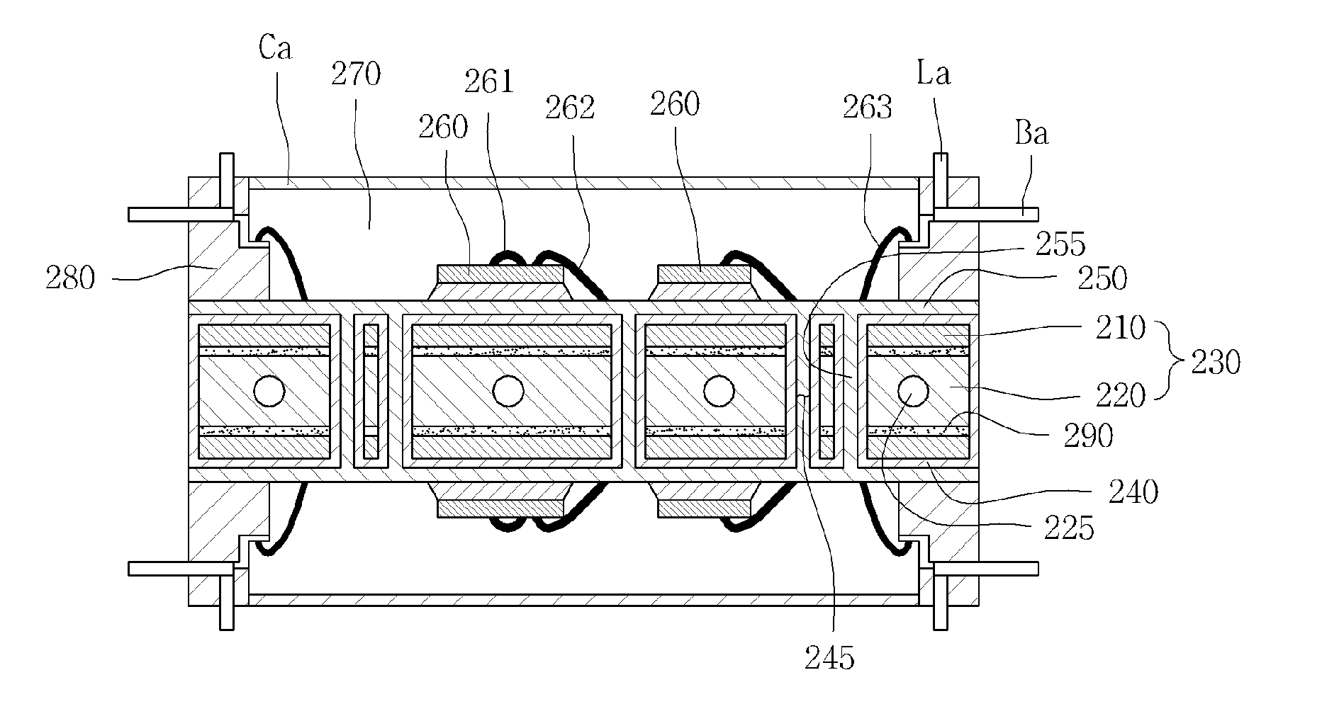
[0040]FIG. 6 is a sectional view illustrating a power semiconductor module, according to a first embodiment of the present invention. The power semiconductor module according to this embodiment will be described below with reference to the drawing.
[0041]As shown in FIG. 6, the power semiconductor module according to this embodiment includes metal plates 110 having anodic oxidation layers 120, a cooling member 130, circuit layers 140...
PUM
 Abstract
Description
Claims
Application Information