Integrated circuit package module and method of the same

Active Publication Date: 2009-12-03
MUTUAL PAK TECH
View PDF1 Cites 7 Cited by
  • Summary
  • Abstract
  • Description
  • Claims
  • Application Information

AI Technical Summary

Benefits of technology

[0006]In light of the foregoing, it is one object of the present invention to provide an integrated circuit module with more external c

Problems solved by technology

However, the integrated circuit module 100 in FIG. 1 has a restricted variety of externa

Method used


Image

  • Integrated circuit package module and method of the same
  • Integrated circuit package module and method of the same
  • Integrated circuit package module and method of the same

Examples


Example

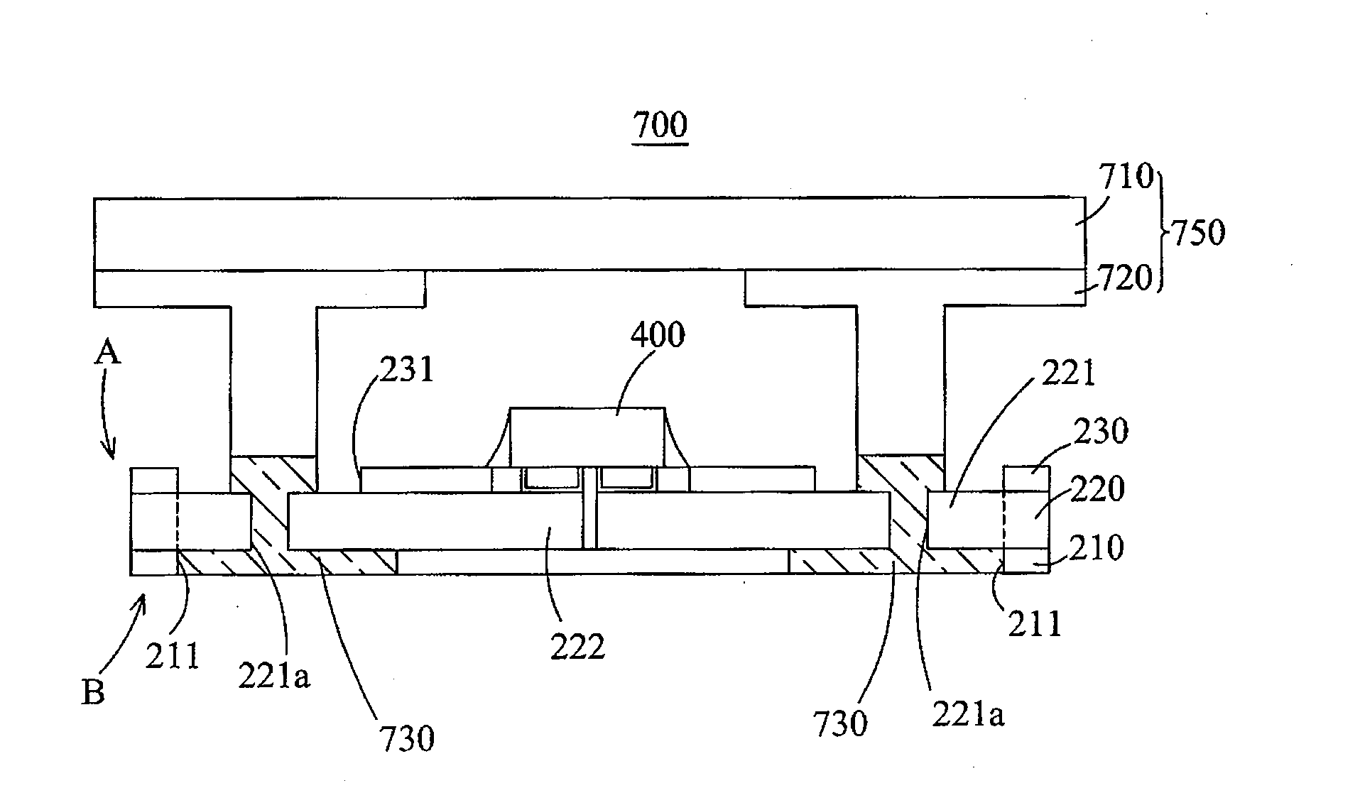
[0021]The preferred embodiments of the present invention will now be described in greater details by referring to the drawings that accompany the present application. It should be noted that the features illustrated in the drawings are not necessarily drawn to scale. Descriptions of well-known components, materials, and process techniques are omitted so as not to unnecessarily obscure the features of the invention.

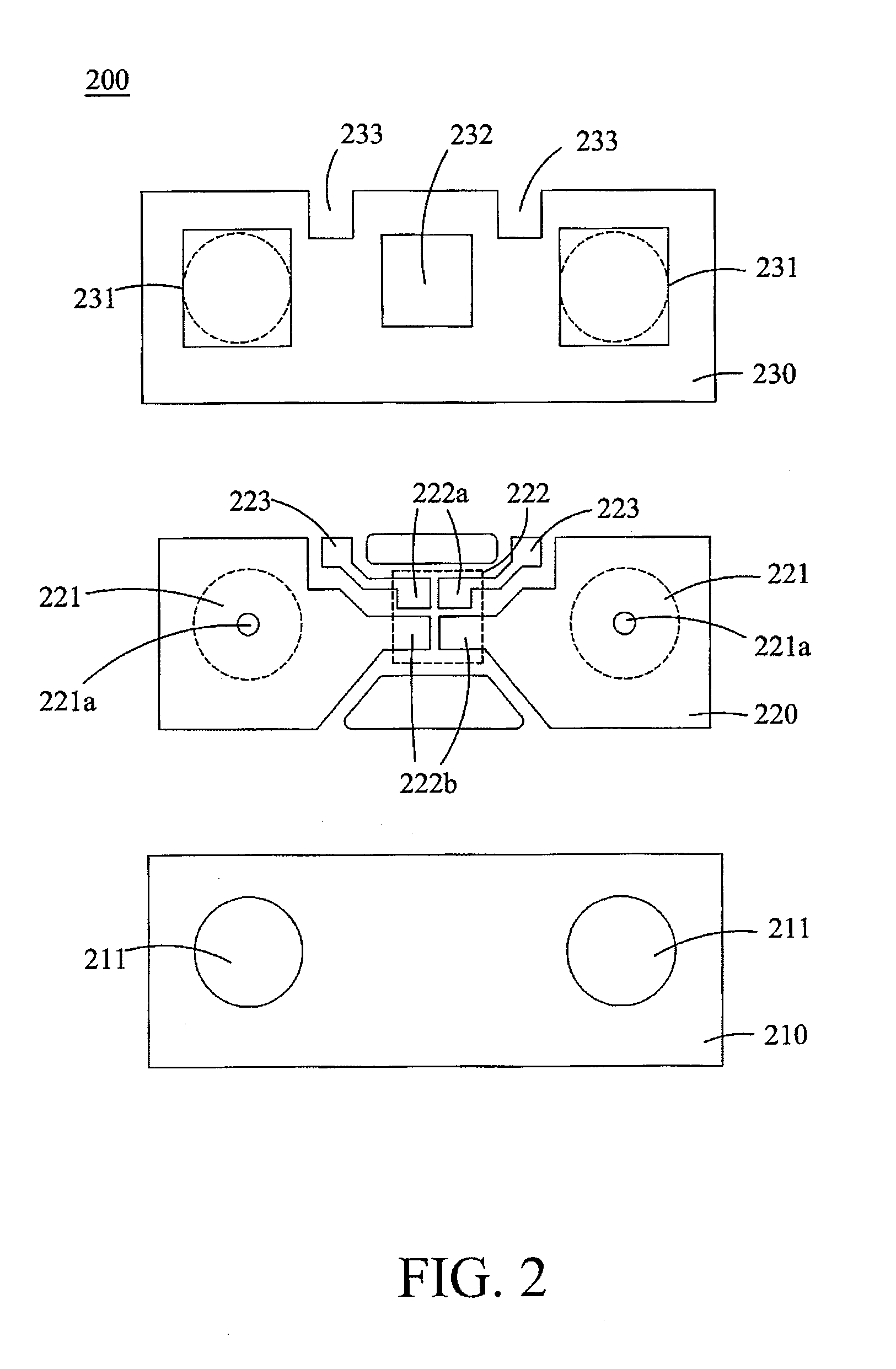
[0022]FIG. 2 shows an explosive view of a carrier 200 supporting a chip in accordance with one embodiment of the present invention, which is used here to illustrate the structure of the carrier 200 and method of the same. As shown in FIG. 2, the method of manufacturing the carrier 200 includes providing a first insulating layer 210. The first insulating layer 210 can be made of polyimide, polyethylene terephthalate, epoxy resin, material of dielectric layer having glass fiber typically used in printed circuit board (such as the glass fiber plate used in FR4), or the combin...


PUM


Abstract

The present invention discloses an integrated circuit module and method of manufacturing the same. The integrated circuit module includes a chip and a carrier supporting the chip. The carrier defines a front side and a back side, and the chip is disposed on the front side. The carrier includes a first insulating layer defining a first opening at the back side, a second insulating layer defining a second opening and a chip accommodation opening at the front side, and a patterned conductive layer sandwiched in between the first insulating layer and the second insulating layer. The patterned conductive layer is formed with an inner contacting portion exposed through the chip accommodation opening and an outer contacting portion exposed through the first opening and the second opening. The inner contacting portion is connected to the chip through the chip accommodation opening. The outer contacting portion is provided for electronically connecting an electronic device to the patterned conductive layer selectively at the front side through the second opening and at the back side through the first opening.

Description

CROSS-REFERENCE TO RELATED APPLICATIONS[0001]This application claims priority to Taiwan Patent Application No. 97120461 entitled “INTEGRATED CIRCUIT PACKAGE MODULE AND METHOD OF THE SAME,” filed on Jun. 2, 2008, which is incorporated herein by reference and assigned to the assignee herein.FIELD OF INVENTION[0002]This invention relates to an integrated circuit package module and method of the same, and more particularly, relates to an integrated circuit package module having a carrier and method of the same.BACKGROUND OF THE INVENTION[0003]Conventionally, external connection for the integrated circuit devices is established by the following steps: mounting a chip on a lead frame; electrically connecting I / O pads of the chip to contacts of the lead frame by wire-bonding; and sealing the chip to complete the package process. Because the lead wires may increase the size of chip package, the wire bonding process is gradually replaced by the leadless packaging technique which can avoid th...

Claims


Application Information

Patent Timeline
IPC IPC(8): H01L23/522H01L21/50
CPCH01L23/49572H01L24/13H01L2924/12041H01L2924/07811H01L2224/133H01L2224/1319H01L2224/73204H01L2224/32225H01L2224/16225H01L2924/01033H01L2924/01005H05K2201/10727H05K2201/10666H01L24/16H01L2224/13099H01L2224/16H01L2924/01029H01L2924/01079H01L2924/01082H01L2924/13091H01L2924/14H01L2924/16195H05K3/321H01L2924/00H01L2924/00014H01L2924/12043
Inventor HWAN, LU-CHENCHEN, PO CHING
Owner MUTUAL PAK TECH
Why Eureka
Try Eureka