Semiconductor device and method of manufacturing semiconductor device
Active Publication Date: 2011-01-20
SHINKO ELECTRIC IND CO LTD
View PDF5 Cites 43 Cited by
Summary
Abstract
Description
Claims
Application Information
AI Technical Summary
This helps you quickly interpret patents by identifying the three key elements:
Problems solved by technology
Method used
Benefits of technology
Benefits of technology
[0024]In one aspect of the invention, the present disclosure provides a semiconductor device and a semiconductor device manufacturing method which a
Problems solved by technology
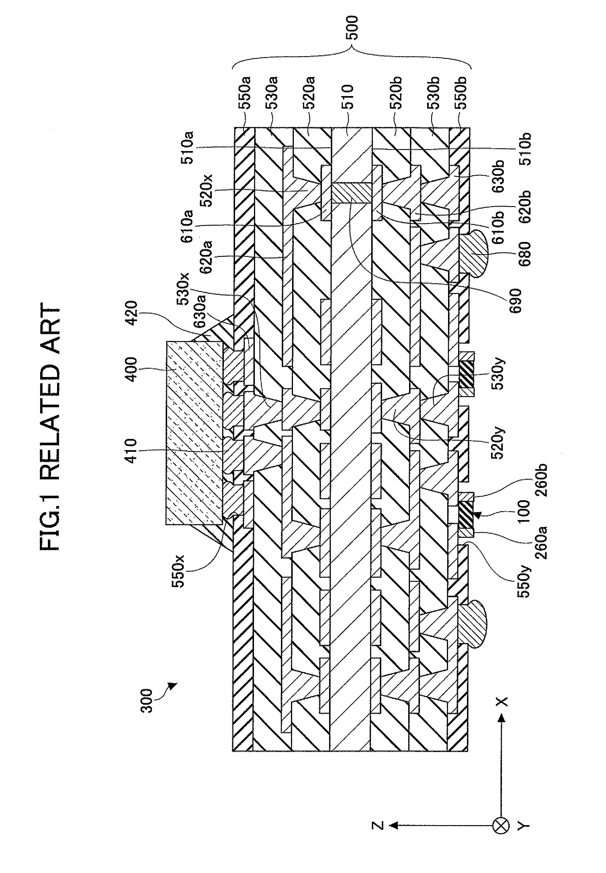
However, in the semiconductor device 300 in which the semiconductor chip is mounted on the substrate, there is a problem in that the reliability of the connection at the portions of the solder bumps 410 where the semiconductor chip 400 and the multi-layer substrate 500 are electrically connected is low.
Hence, it is difficult to attain high-density fabrication of the semiconductor device 700.
Method used
Image
Click on the blue label to locate the original text in one second.
Reading with bidirectional positioning of images and text.
Examples
first embodiment
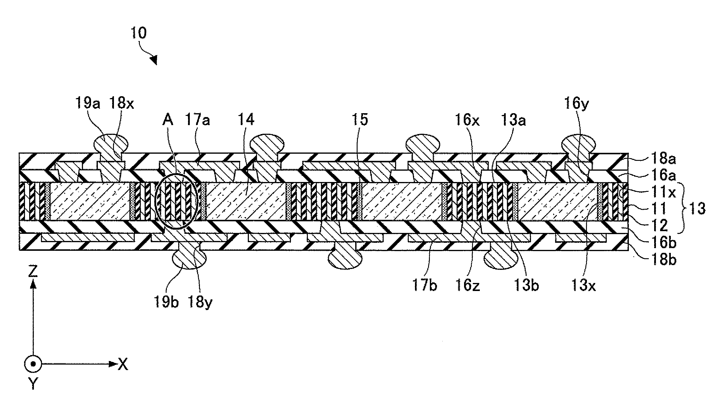
[0050]As illustrated in FIG. 3 and FIG. 4, the semiconductor device 10 of the first embodiment includes a substrate 13, a semiconductor chip 14, an insulating resin 15, a first insulating layer 16a, a second insulating layer 16b, a first wiring layer 17a, a second wiring layer 17b, a first solder resist layer 18a, a second solder resist layer 18b, a first solder bump 19a, and a second solder bump 19b.
[0051]In the semiconductor device 10, the substrate 13 is, for example, a substrate having a thickness in a range of 70-100 micrometers and a size of about 10×10 mm. This substrate 13 includes an insulating base material 11 in which a large number of through holes 11x extending in the direction Z (the thickness direction) are formed in the whole area thereof, and these through holes 11x are filled up with a metallic material to form a large number of line conductors (vias) 12. Examples of the insulating base material 11 may include alumina (aluminum oxide), mullite, aluminum nitride, c...
second embodiment
[0109]Next, FIG. 17 is a cross-sectional view of a semiconductor device of the present disclosure. In FIG. 17, the elements which are the same as corresponding elements of the semiconductor device 10 in FIG. 3 are designated by the same reference numerals, and a description thereof will be omitted.
[0110]In FIG. 17, the direction X indicates a direction which is parallel to one surface 13a of the substrate 13, the direction Y indicates a direction (or a width direction of the substrate 13) which is perpendicular to the direction X and parallel to one surface 13a of the substrate 13, and the direction Z indicates a direction (or a thickness direction of the substrate 13) which is perpendicular to both the direction X and the direction Y.
[0111]As illustrated in FIG. 17, the semiconductor device 30 of the second embodiment has a structure which is essentially the same as that of the semiconductor device 10 of the first embodiment but differs in that one of a plurality of semiconductor c...
third embodiment
[0116]Next, FIG. 18 is a cross-sectional view of a semiconductor device of the present disclosure. In FIG. 18, the elements which are the same as corresponding elements of the semiconductor device 10 in FIG. 3 are designated by the same reference numerals, and a description thereof will be omitted.
[0117]In FIG. 18, the direction X indicates a direction which is parallel to one surface 13a of the substrate 13, the direction Y indicates a direction (or a width direction of the substrate 13) which is perpendicular to the direction X and parallel to one surface 13a of the substrate 13, and the direction Z indicates a direction (or a thickness direction of the substrate 13) which is perpendicular to both the direction X and the direction Y.
[0118]As illustrated in FIG. 18, the semiconductor device 40 of the third embodiment has the structure which is essentially the same as that of the semiconductor device 10 of the first embodiment but differs in that two semiconductor chips 14 are arran...
PUM
Abstract
In a semiconductor device, a substrate includes a plurality of line conductors which penetrate the substrate from a top surface to a bottom surface of the substrate. A semiconductorchip is secured in a hole of the substrate. A first insulating layer is formed on the top surfaces of the substrate and the semiconductorchip. A first wiring layer is formed on the first insulating layer and electrically connected via through holes of the first insulating layer to the semiconductor chip and some line conductors exposed to one of the through holes. A second insulating layer is formed on the bottom surfaces of the substrate and the semiconductor chip. A second wiring layer is formed on the second insulating layer and electrically connected via a through hole of the second insulating layer to some line conductors exposed to the through hole.
Description
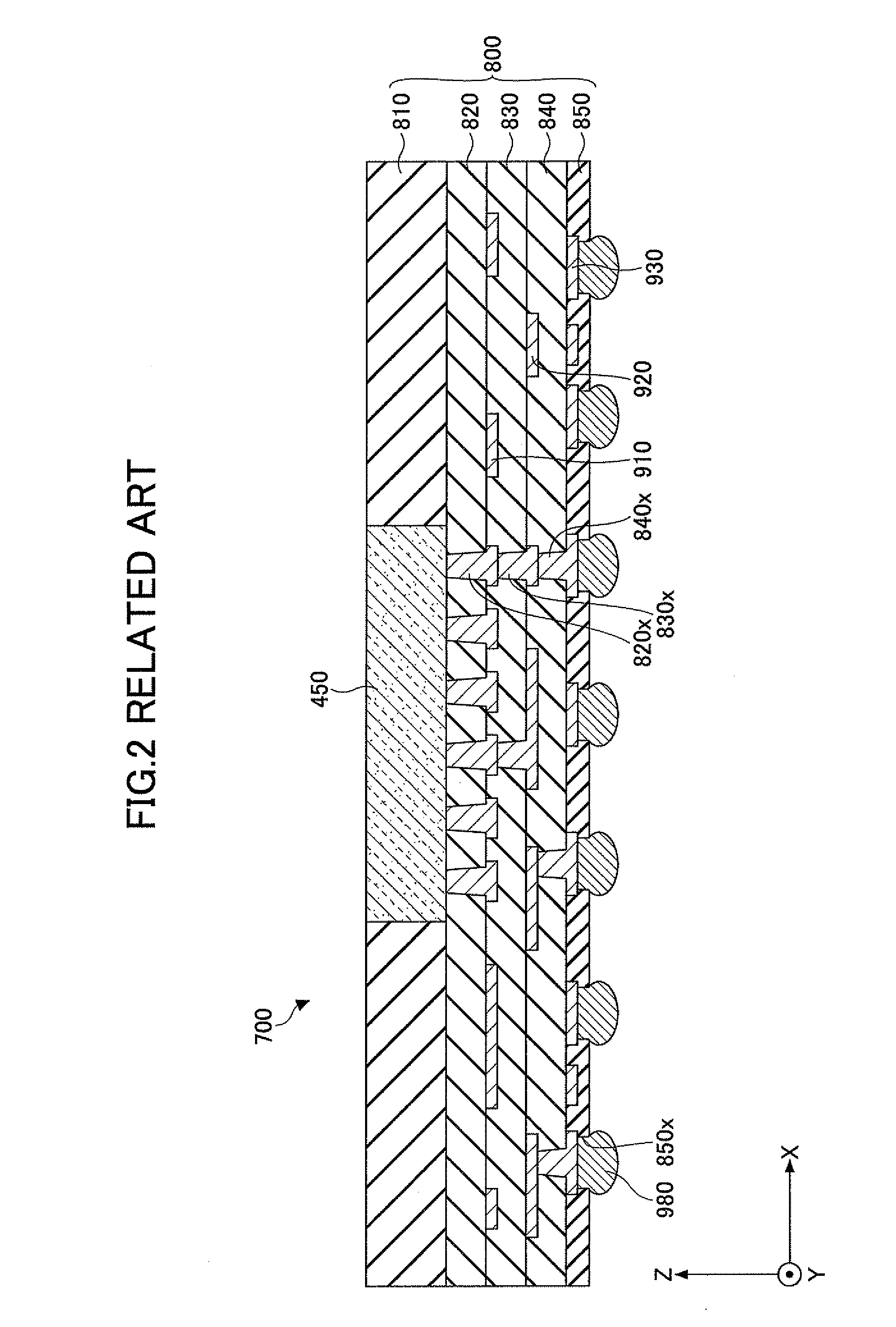
CROSS-REFERENCE TO RELATED APPLICATION[0001]This application is based upon and claims the benefit of priority of Japanese patent application No. 2009-168596, filed on Jul. 17, 2009, the entire contents of which are incorporated herein by reference in their entirety.BACKGROUND OF THE INVENTION[0002]1. Field of the Invention[0003]This invention relates to a semiconductor device containing a semiconductor chip and a substrate, and relates to a method of manufacturing a semiconductor device containing a semiconductor chip and a substrate.[0004]2. Description of the Related Art[0005]Conventionally, a semiconductor device in which a semiconductor chip is mounted on a substrate is known. Referring to FIG. 1, a semiconductor device according to the related art in which a semiconductor chip is mounted on a substrate will be described.[0006]FIG. 1 is a cross-sectional view of a semiconductor device according to the related art in which a semiconductor chip is mounted on a substrate. As illust...
Claims
Application Information
Patent Timeline
Application Date:The date an application was filed.
Publication Date:The date a patent or application was officially published.
First Publication Date:The earliest publication date of a patent with the same application number.
Issue Date:Publication date of the patent grant document.
PCT Entry Date:The Entry date of PCT National Phase.
Estimated Expiry Date:The statutory expiry date of a patent right according to the Patent Law, and it is the longest term of protection that the patent right can achieve without the termination of the patent right due to other reasons(Term extension factor has been taken into account ).
Invalid Date:Actual expiry date is based on effective date or publication date of legal transaction data of invalid patent.

