Hybrid multilayer substrate and method for manufacturing the same

a multi-layer substrate and hybrid technology, applied in the direction of transportation and packaging, chemistry apparatus and processes, association of printed circuit non-printed electric components, etc., can solve the problems of difficult to obtain electrical conduction between the ic chip and the electrodes provided in the resin insulating layer, and the terminal electrodes cannot be easily and accurately provided, so as to improve the positional accuracy of the terminal electrodes and improve the reliability of connection

Active Publication Date: 2007-08-02
MURATA MFG CO LTD
View PDF3 Cites 28 Cited by
  • Summary
  • Abstract
  • Description
  • Claims
  • Application Information

AI Technical Summary

Benefits of technology

[0009] To overcome the problems described above, preferred embodiments of the present invention provide a hybrid multilayer substrate and a method for manufacturing the same, the hybrid multilayer substrate having improved positional accuracy of the terminal electrodes provided in the bottom surface of the cavity and being capable of significantly improving the reliability in connection with a mounted component.

Problems solved by technology

However, with the wiring substrate disclosed in Patent Document 1, since the resin insulating layer having via holes is provided for the IC chip fixed in the penetrating hole of the ceramic core substrate by the filling material, and a self-alignment function of the IC chip cannot be used during mounting, terminals of the IC chip and the via holes (electrodes) of the resin insulating layer cannot be easily and accurately provided, and as a result, it is difficult to obtain electrical conduction between the IC chip and the electrodes provided in the resin insulating layer.
As a result, it is increasingly difficult to obtain electrical conduction between the IC chip and the electrodes provided in the resin insulating layer.
However, as shown in FIG. 11, when the resin insulating layer 2 is bonded to the ceramic substrate 1 by thermocompression bonding, the resin insulating layer 2 flows during the thermocompression bonding, the electrodes 2A located in the cavity 3 are shifted in the horizontal direction thereby, and thus, it is difficult to form the electrodes 2A with high accuracy.
This tendency becomes more apparent as the number of films which define the resin insulating layer 2 is increased, and as a result, the reliability of connection may not be satisfactory in some cases.

Method used


Image

  • Hybrid multilayer substrate and method for manufacturing the same
  • Hybrid multilayer substrate and method for manufacturing the same
  • Hybrid multilayer substrate and method for manufacturing the same

Examples


Embodiment Construction

[0039] Hereinafter, the present invention will be described with reference to preferred embodiments shown in FIGS. 1A to 10.

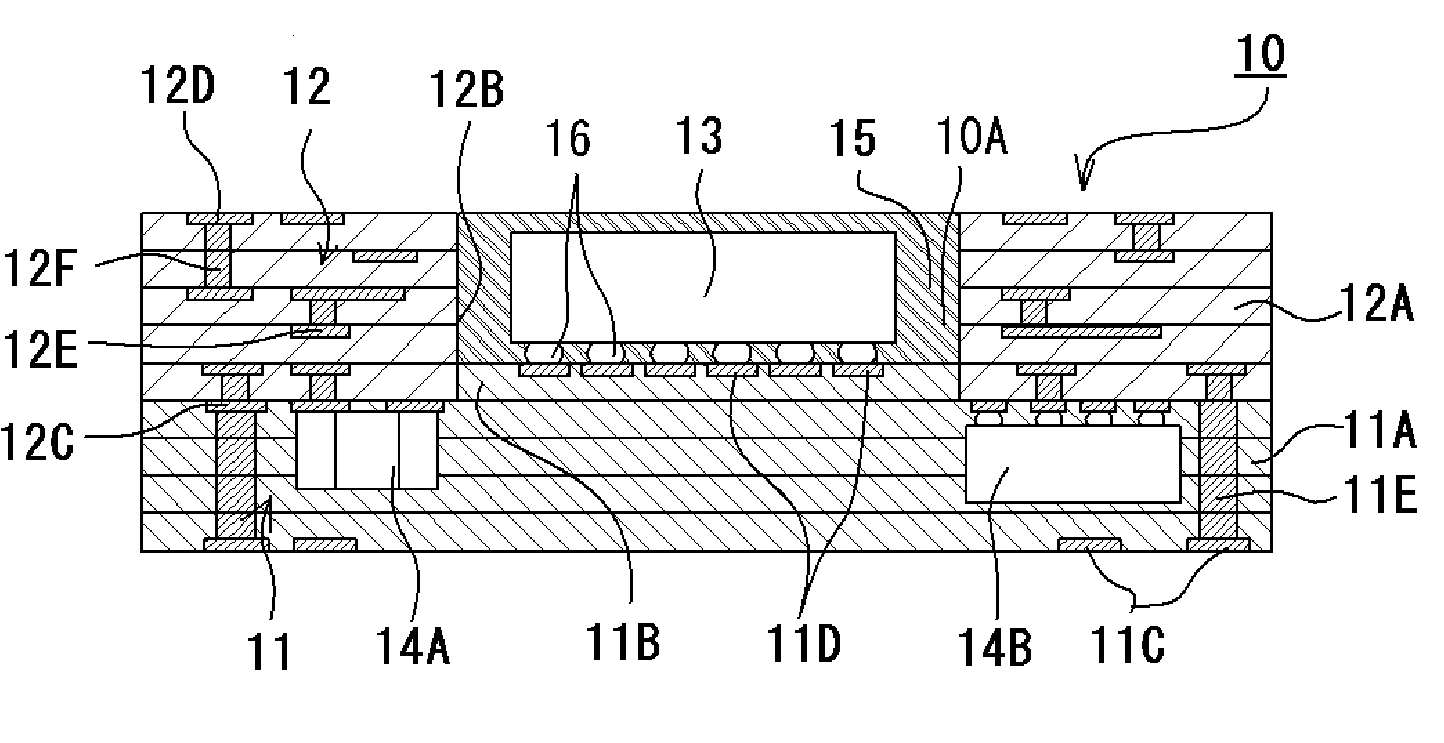
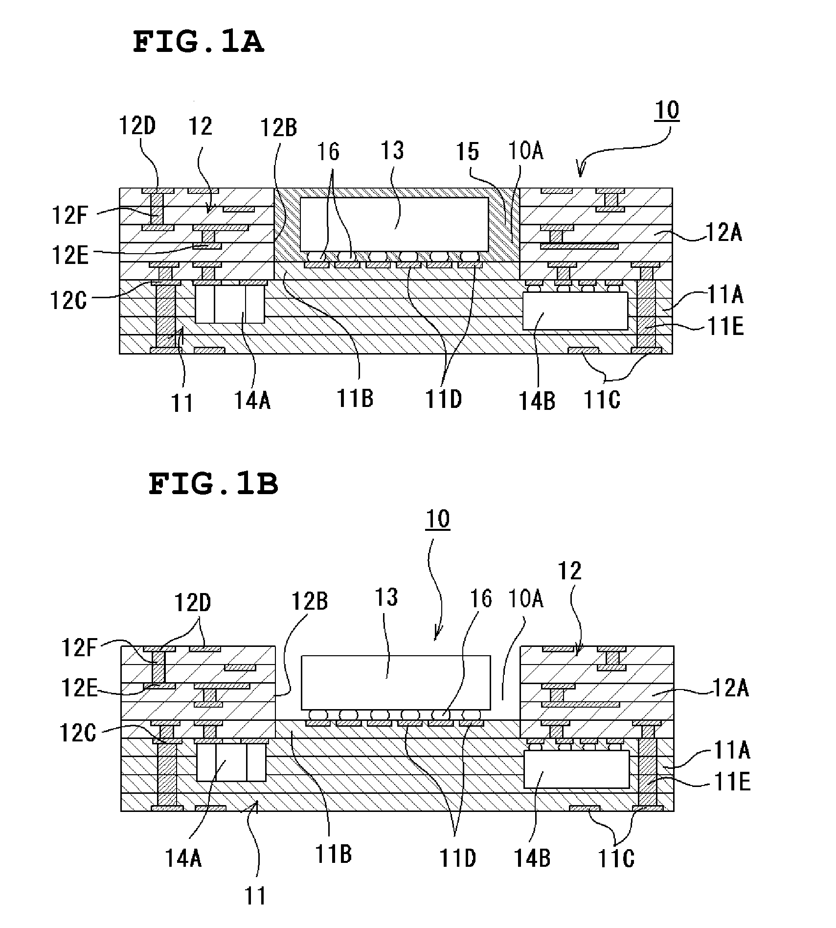
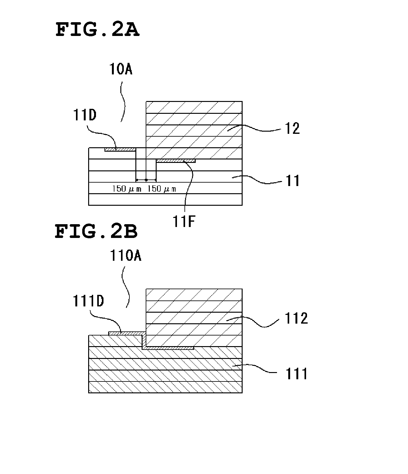
[0040] A hybrid multilayer substrate 10 of this preferred embodiment includes, as shown in FIG. 1A by way of example, a cavity 10A in a laminate structure which includes a resin portion 11 and a ceramic substrate 12 laminated thereon, and is mounted on a mounting substrate (not shown), such as a printed circuit board, with the resin portion 11 provided therebetween. In addition, when the hybrid multilayer substrate 10 is mounted on a ceramic-made substrate, mounting may be performed with the ceramic substrate 12 provided therebetween. Since the mounting substrate, such as a printed circuit board, is made of a resin in many cases, the resin portion 11 is preferably made of a resin having a thermal expansion coefficient between the thermal expansion coefficient of the ceramic substrate 12 and that of the mounting substrate, such as an intermediate thermal expans...


PUM

PropertyMeasurementUnit
heightaaaaaaaaaa
heightaaaaaaaaaa
heightaaaaaaaaaa

Abstract

A hybrid multilayer substrate includes a cavity in a laminate structure formed of a resin portion and a ceramic multilayer substrate, the resin portion has a protrusion portion, the ceramic multilayer substrate has a penetrating hole, and the cavity is formed by fitting the protrusion portion of the resin portion to an end portion of the penetrating hole of the ceramic multilayer substrate.

Description

BACKGROUND OF THE INVENTION [0001] 1. Field of the Invention [0002] The present invention relates to hybrid multilayer substrates and methods for manufacturing the same, and more particularly, to a highly reliable hybrid multilayer substrate having a cavity in which an electronic component is mounted with high accuracy, and to a method for manufacturing the hybrid multilayer substrate. [0003] 2. Description of the Related Art [0004] A related wiring substrate having a cavity is disclosed in Japanese Unexamined Patent Application Publication No. 2003-309213 (Patent Document 1). This wiring substrate includes a ceramic core substrate having a penetrating hole, a resin insulating layer which is provided on the bottom surface of this ceramic core substrate and which blocks the penetrating hole so as to define a cavity, an IC chip mounted in the cavity defined by the resin insulating layer, and a filling material which is filled around the IC chip to seal it in the cavity. [0005] When th...

Claims


Application Information

Patent Timeline
Patent Type & Authority Applications(United States)
IPC IPC(8): B32B3/10
CPCH01L23/5389Y10T428/24917H01L25/0652H01L25/16H01L25/50H01L2224/16225H01L2224/48091H01L2224/48227H01L2224/75315H01L2924/01004H01L2924/01013H01L2924/01029H01L2924/01033H01L2924/01047H01L2924/01061H01L2924/01078H01L2924/01079H01L2924/01082H01L2924/09701H01L2924/15153H01L2924/1517H01L2924/19041H01L2924/19105H05K1/0306H05K1/0313H05K1/183H05K1/186H05K3/284H05K3/4614H05K3/4688H05K3/4697H05K2203/061H05K2203/063H05K2203/167H01L24/75Y10T428/24322Y10T428/24331H01L2924/12041H01L24/48H01L2924/01005H01L2924/01006H01L2924/00014H01L2924/00H01L2924/12042H01L2924/14H01L2924/15787H01L2924/181H01L2924/00012H01L2224/45099H01L2224/45015H01L2924/207
Inventor OGAWA, NOBUAKINISHIZAWA, YOSHIHIKO
Owner MURATA MFG CO LTD
Why Eureka
Try Eureka