

Reflection-type exposure mask and method of manufacturing a semiconductor device
a semiconductor device and exposure mask technology, applied in the field of reflection-type exposure masks and manufacturing semiconductor devices, can solve the problems of difficult to form an optical image having an adequate contrast value on the wafer, and achieve the effect of high reflective regions
- Summary
- Abstract
- Description
- Claims
- Application Information
AI Technical Summary
Benefits of technology
Problems solved by technology
Method used
Image

Examples
Embodiment Construction
[0024]An embodiment of the invention will now be described with reference to the accompanying drawings.
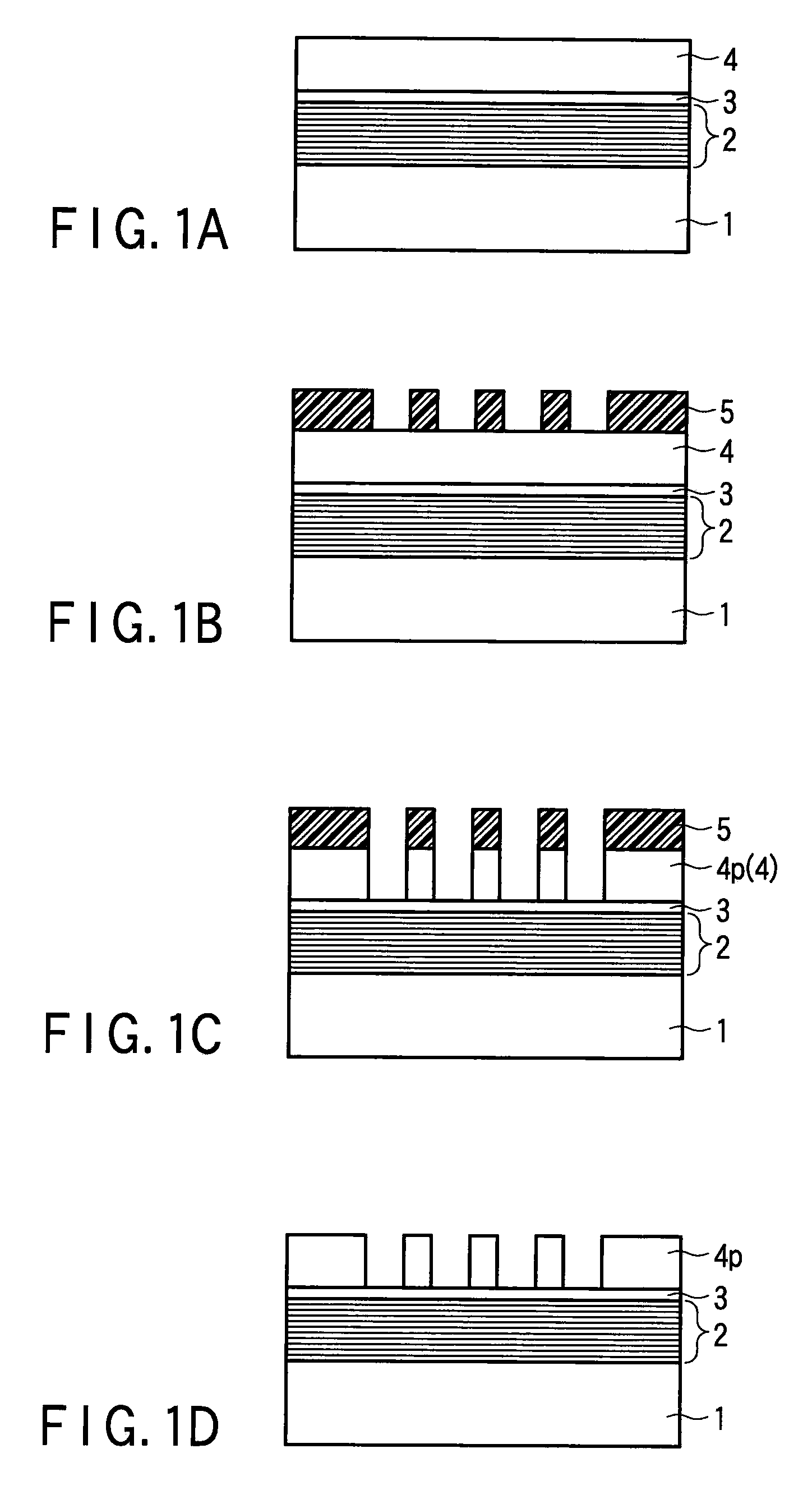
[0025]FIG. 1A to FIG. 1D are cross-sectional views for describing a method of manufacturing a reflection-type exposure mask according to the present embodiment.
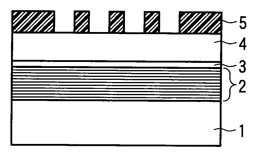
[0026][FIG. 1A]
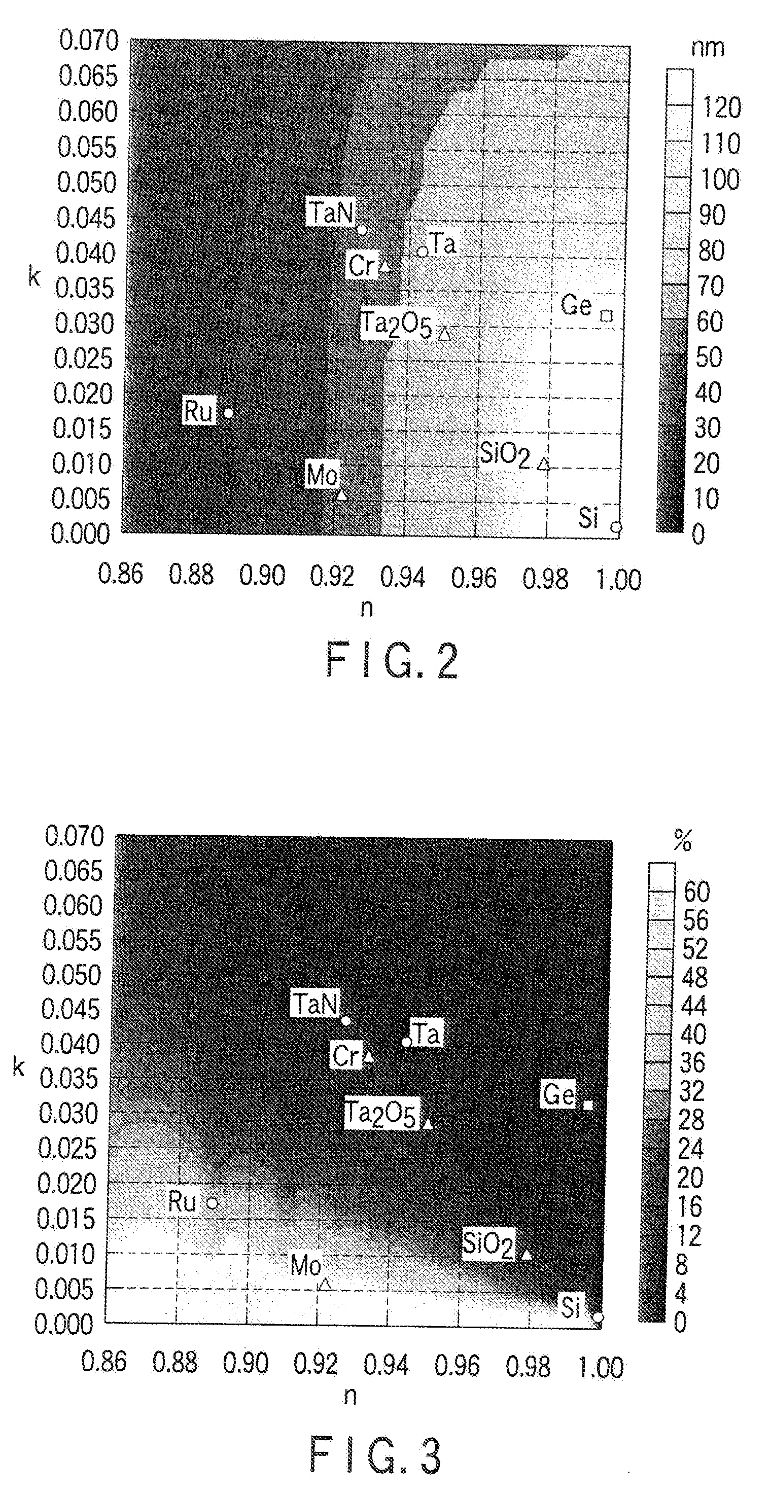
[0027]A multilayer reflection film 2 (high reflection region) which reflects EUV (exposure light), is formed on a glass substrate 1 having low thermal expansion coefficient. The multiplayer reflection film 2 is configured such that a plurality of pairs of a Mo film and a Si film which are stacked. In the present embodiment, the number of pairs of a Mo film and a Si film is 40, the thickness of the No film is 2.8 nm, and the thickness of the Si film is 4.2 nm. In addition, in the present embodiment, the main surface (surface to be irradiated with exposure light) of the glass substrate 1 is the surface on which the multilayer reflection film 2 is formed (i.e. the top surface of the glass substrate 1 shown in FIG...
PUM
| Property | Measurement | Unit |
|---|---|---|
| thickness | aaaaa | aaaaa |
| thickness | aaaaa | aaaaa |
| reflectance ratio | aaaaa | aaaaa |
Abstract
Description
Claims
Application Information