
Cooling apparatus for semiconductor component

Inactive Publication Date: 2011-02-03
ADD BLUE CORP
View PDF1 Cites 2 Cited by
  • Summary
  • Abstract
  • Description
  • Claims
  • Application Information

AI Technical Summary

Benefits of technology

[0011]In order to solve the above-mentioned problems, it is an object of the present invention to provide a cooling apparatus for a semiconductor component having an optimal coolant inlet flow path structure capable of improving cooling efficiency and reducing resistance to coolant flow.
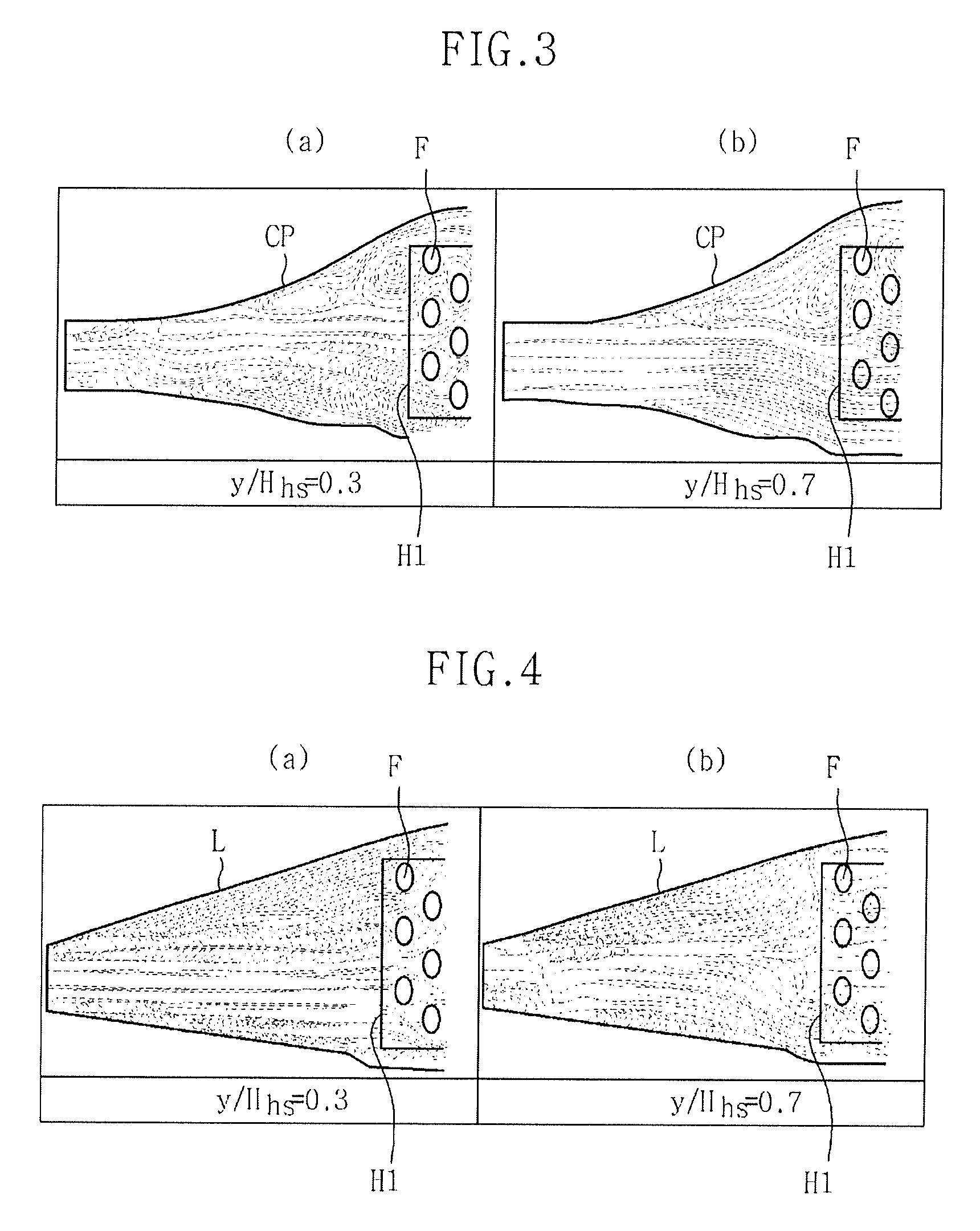
[0022]In the cooling apparatus for compact and integrated semiconductor components according to the embodiment of the present invention, since the diffuser-shaped coolant inlet flow path extending from the coolant inlet to the cooling fins is designed in an optimal shape, it is possible to improve cooling efficiency and to reduce resistance to coolant flow.

Problems solved by technology

With the recent requirements of compact design and improvement in the degree of integration of various elements of electronic components, power consumed by each component increases and high heat is generated in electronic elements.
If heat generated in a semiconductor component during operation is not appropriately dissipated, the life time of the component may decrease while the performance of the component is rapidly deteriorated, and furthermore, the whole system may become damaged.
However, in this case, since reserve flow and vortex occurs, the effect is less dominant in improving cooling efficiency and reducing resistance to coolant flow.
For this reason, it is difficult to form a coolant inlet flow path having a high cooling efficiency and small resistance to flow.

Method used


Image

  • Cooling apparatus for semiconductor component
  • Cooling apparatus for semiconductor component
  • Cooling apparatus for semiconductor component

Examples


Embodiment Construction

[0031]Hereinafter, exemplary embodiments of the present invention will be described with reference to the accompanying drawings.

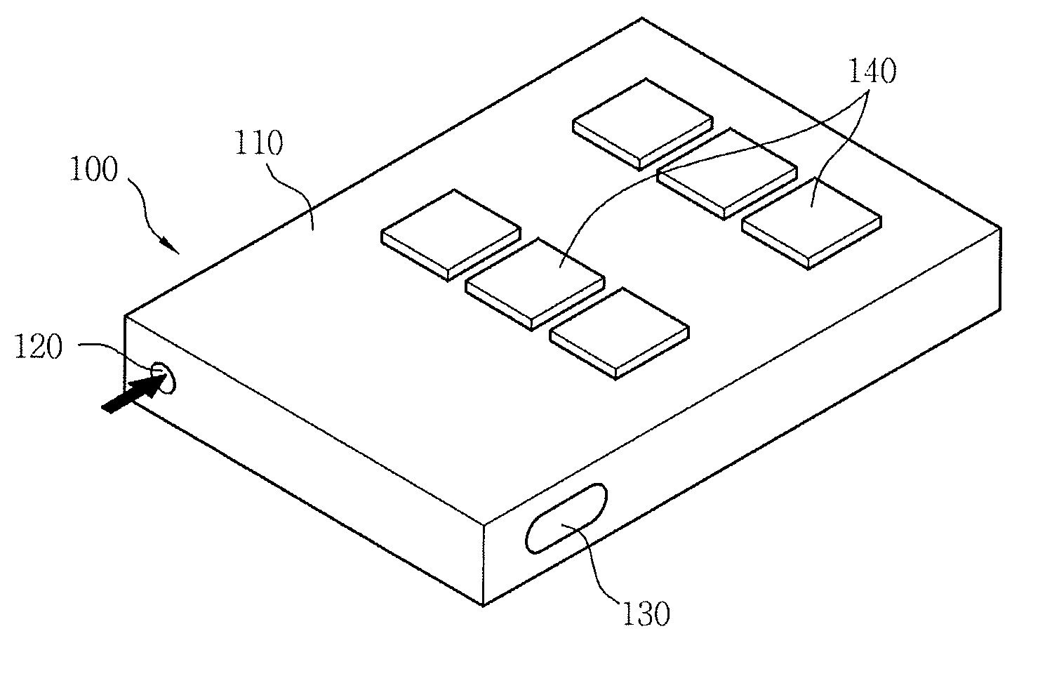
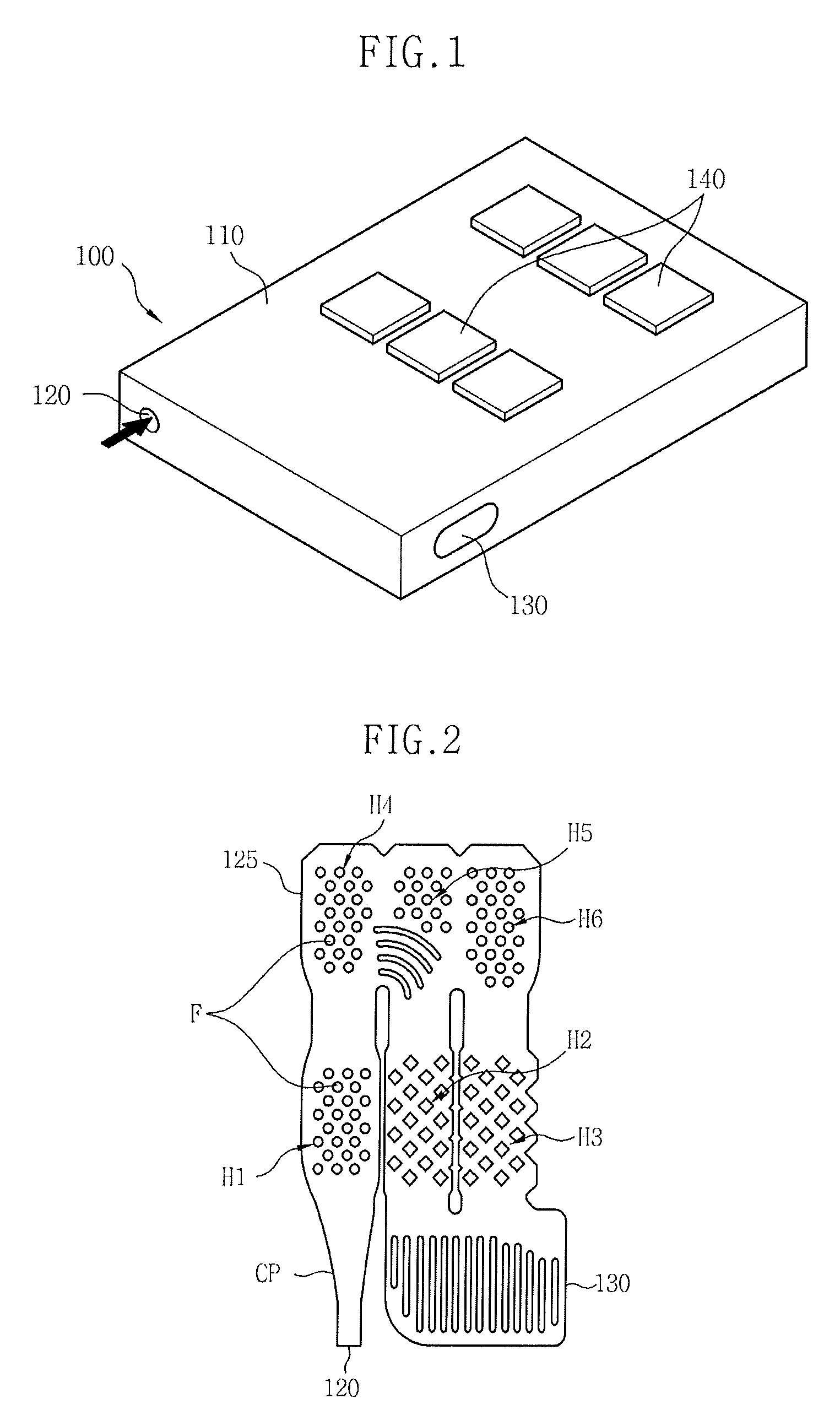
[0032]FIG. 1 is a perspective view schematically illustrating a cooling apparatus for semiconductor components according to an exemplary embodiment of the present invention. FIG. 2 is a planar cross-sectional view illustrating the internal of the cooling apparatus in shown FIG. 1. As shown in the drawings, a cooling apparatus 100 has a coolant inlet 120 formed on one side of a main body 110, an coolant outlet 130 formed on another side of the main body 110, and a coolant flow path 125 connecting the coolant inlet 120 and the coolant outlet 130. A number of semiconductor components 140 are attached to the top surface of the main body 110.

[0033]Inside the main body 110, as shown in FIG. 2, a coolant flow path 125 is formed to extend from the coolant inlet 120 to the coolant outlet 130. In the coolant flow path 125, there are provided a number of heat sinks H1...


PUM


Abstract

Disclosed is a cooling apparatus for a semiconductor component having a coolant inlet flow path on a coolant flow path connecting a coolant inlet and a coolant outlet, the coolant inlet flow path having a diffuser shape, in which its cross-sectional area increases from a coolant inlet to a portion where cooling fins start to appear. In the cooling apparatus, the coolant inlet flow path meets the following equation:ω=D{3 / 2+sin(α(x−A))}.Here, ω is the radius of the diffuser, D is the diameter of the coolant inlet, x is a distance from the coolant inlet toward the cooling fins, α is an expansion slope coefficient of the diffuser in radians, and the sine of (α·A) is 1.In the cooling apparatus for a compact and integrated semiconductor component, since the diffuser-shaped coolant inlet flow path extending from the coolant inlet to the cooling fins is designed in an optimal shape, it is possible to improve cooling efficiency and to reduce flow resistance to coolant flow.

Description

BACKGROUND OF THE INVENTION[0001]1. Field of the Invention[0002]The present invention relates to a cooling apparatus for semiconductor components, and more particularly, to a cooling apparatus for semiconductor components having an optimal coolant inlet flow path structure capable of improving cooling efficiency and reducing resistance to coolant flow. This application claims priority from Korean Patent Application No. 10-2009-0069794 on Jul. 30, 2009 in the Korean Intellectual Property Office (KIPO), the disclosure of which is incorporated herein by reference in its entirety.[0003]2. Description of the Related Art[0004]With the recent requirements of compact design and improvement in the degree of integration of various elements of electronic components, power consumed by each component increases and high heat is generated in electronic elements. If heat generated in a semiconductor component during operation is not appropriately dissipated, the life time of the component may decre...

Claims


Application Information

Patent Timeline
IPC IPC(8): F28D15/00
CPCF28D2021/0029F28F3/042H01L23/473H01L2924/0002H01L2924/00H01L23/34F28D15/02
Inventor KIM, JAEWON
Owner ADD BLUE CORP
Learn More