Non-contact IC tag

a technology of ic tags and resonant antennas, applied in the structural forms of radiating elements, instruments, resonant antennas, etc., can solve the problems of short communication distance, ensuring long distance communication, and supply of electric power, and achieve the effect of increasing communication distan

Inactive Publication Date: 2011-02-03
TORAY IND INC
View PDF4 Cites 11 Cited by
  • Summary
  • Abstract
  • Description
  • Claims
  • Application Information

AI Technical Summary

Benefits of technology

[0031]If a non-contact IC tag according to an embodiment of the invention is used, normal communication can be maintained between the non-contact IC tag and a reader/writer even when the non-contact IC tag is attached to a metal member. If the non-contact IC tag according to an embodiment of the invention is used, a larger electric power is supplied to an IC chip containe

Problems solved by technology

However, in the IC tags (1) and (2), it is difficult to supply electric power to the IC chip, leading to a short communication distance, which is a problem.
In the IC tag (3), the resin has to be thick to ensure a long communication distance, leading t

Method used


Image

  • Non-contact IC tag
  • Non-contact IC tag
  • Non-contact IC tag

Examples


example 1

[0100]A bi-axially stretched polyethylene terephthalate film (Lumiror (registered trademark) S10 supplied by Toray Industries, Inc.) having a thickness of 0.05 mm was used as the first insulating substrate 2. To produce a metallized film, an aluminum layer having a thickness of 0.002 mm was formed by electron beam (EB) deposition over one side of the first insulating substrate 2.

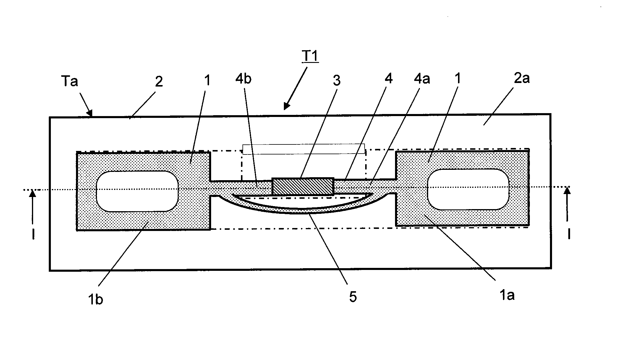
[0101]The resulting metallized film was subjected to wet etching to produce a parasitic antenna having a shape as shown in FIG. 3. The sizes shown in FIG. 3 were as described below: a=8 mm, b=97 mm, c=43.5 mm, d=4 mm, and e=10 mm. The first parasitic antenna 6, second parasitic antenna 7, and connected portion 8 were thus formed.

[0102]A UHF tag Ta (ALN-9540-Squiggle supplied by Alien) having an IC chip 3 and a matching-circuit equipped dipole antenna 1 was prepared. An acrylic plate having a thickness of 1 mm was used as a second insulating substrate 9, and the UHF tag Ta was adhered to it. Then, the first s...

example 2

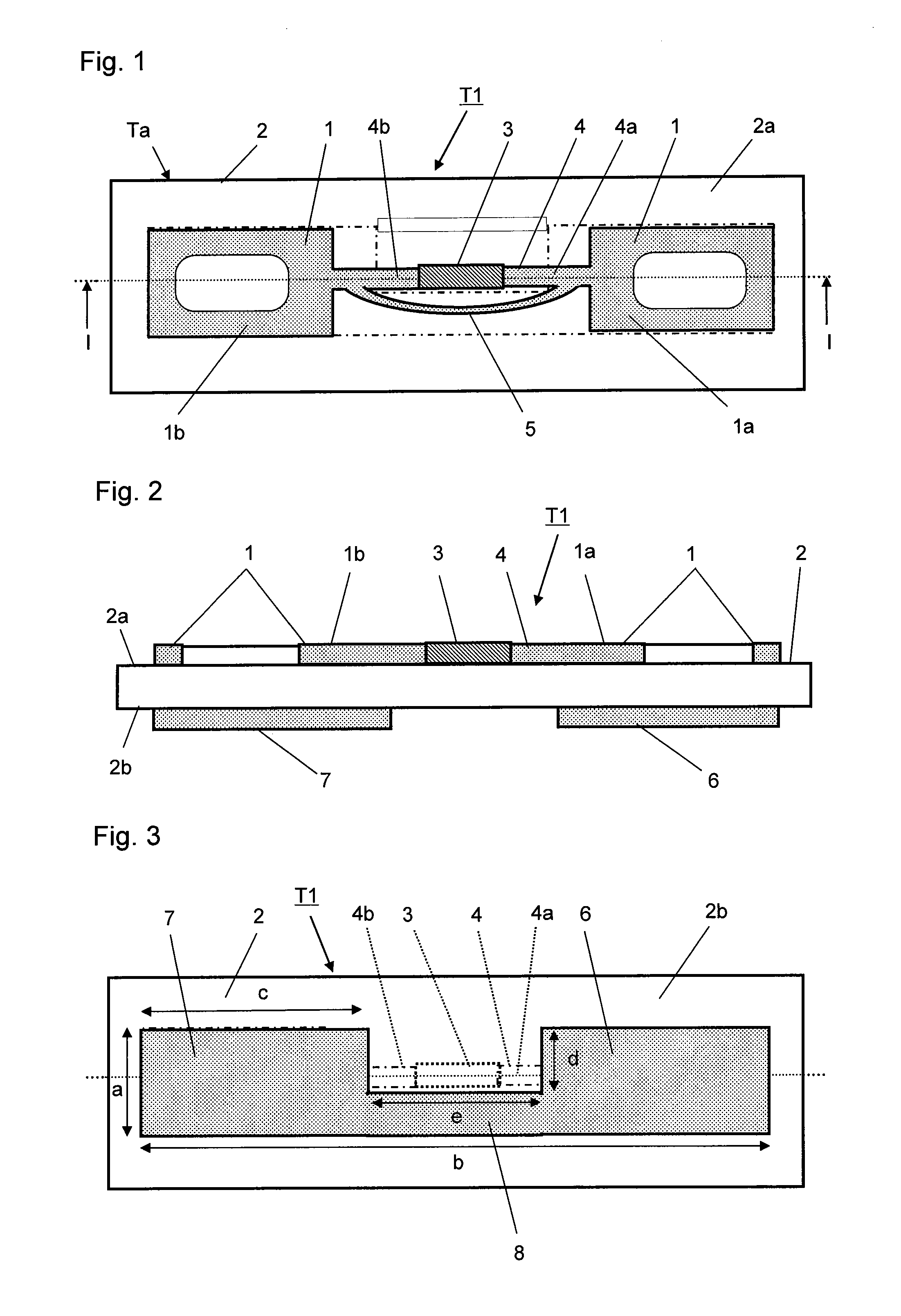
[0108]The metallized film obtained in Example 1 was subjected to wet etching to produce a parasitic antenna having a shape as shown in FIG. 4. The sizes shown in FIG. 4 were as described below: a=8 mm, b=97 mm, c=43.5 mm, d=4 mm, and e=10 mm. The first parasitic antenna 6, the second parasitic antenna 7, and the connected portion 8 were thus formed. The resulting metallized film and the second insulating substrate produced in Example 1 were fixed together by the same procedure as in Example 1 to provide a non-contact IC tag T2.

[0109]The resulting non-contact IC tag T2 had a communication distance of 690 mm.

example 3

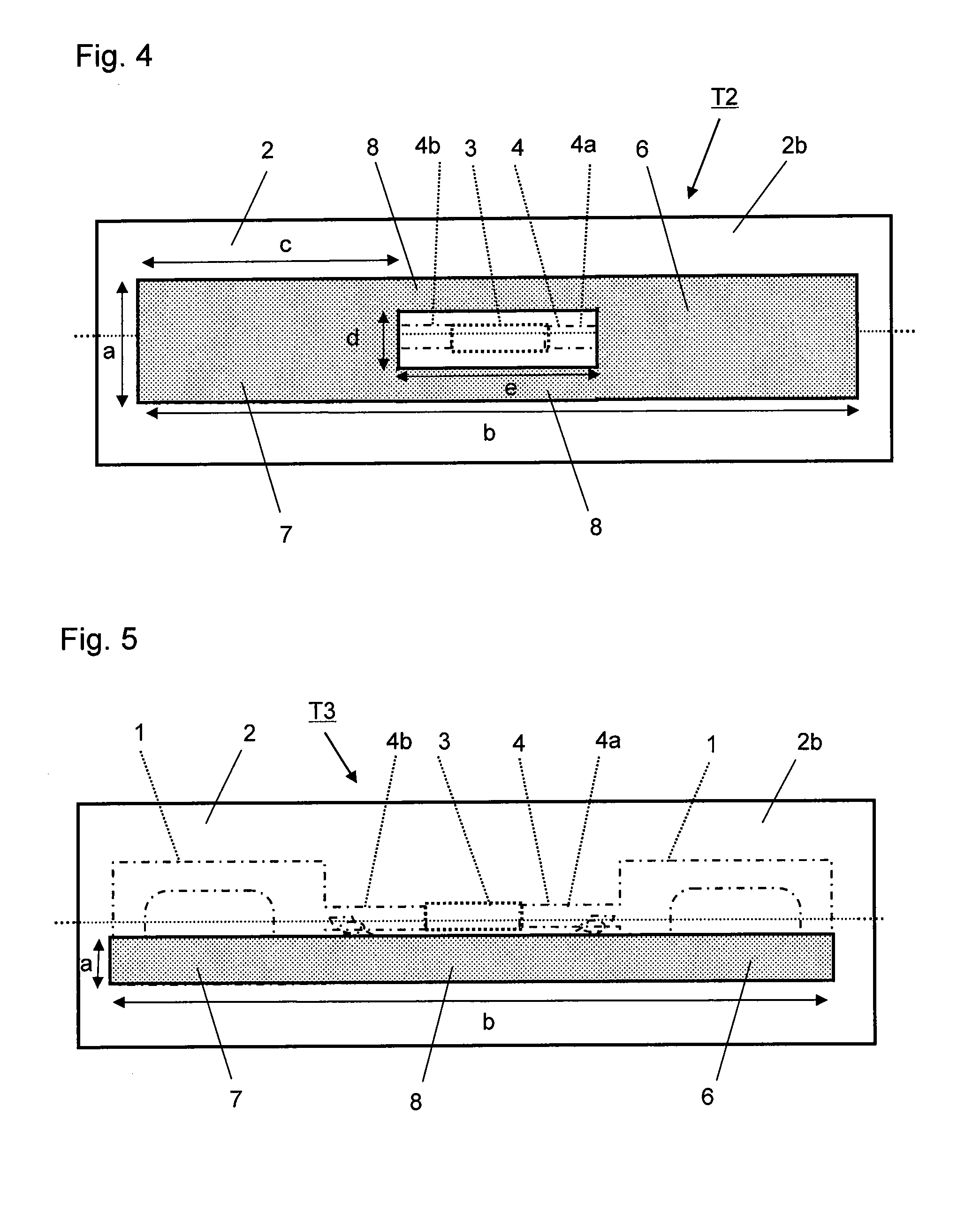
[0110]The metallized film obtained in Example 1 was subjected to wet etching to produce a parasitic antenna having a shape as shown in FIG. 5. The sizes shown in FIG. 5 were as described below: a=4 mm and b=97 mm. The first parasitic antenna 6, the second parasitic antenna 7, and the connected portion 8 were thus formed. The resulting metallized film and the second insulating substrate produced in Example 1 were fixed together by the same procedure as in Example 1 to provide a non-contact IC tag T3.

[0111]The resulting non-contact IC tag T3 had a communication distance of 790 mm.


PUM


Abstract

A non-contact IC tag includes an insulating substrate, an IC tag having an IC chip and a matching-circuit equipped dipole antenna connected with the IC chip, and a first and second parasitic antenna both provided at the other side of the insulating substrate. The matching-circuit equipped dipole antenna has two antenna sections, a connecting terminal section and a matching circuit section. Projection images of the first and second parasitic antennae onto the one side of the insulating substrate respectively overlap at least portions of the two antenna sections of the matching-circuit equipped dipole antenna. The first and second parasitic antennae are made electrically conductive by a connected portion, and the projection images of the first and second parasitic antennae, and the connected portion onto the one side of the insulating substrate do not overlap the IC chip and the connecting terminal section of the matching-circuit equipped dipole antenna.

Description

FIELD OF THE INVENTION[0001]The present invention relates to a non-contact IC tag. The invention relates to a non-contact IC tag whose communication performance is little influenced by a metal member to which it is stuck. In particular, the invention relates to a passive-type non-contact IC tag that uses radio wave (microwave) to achieve transmission.BACKGROUND OF THE INVENTION[0002]A non-contact IC tag comprises an antenna circuit and an IC chip (chip with a built-in integrated circuit) that stores required information. A non-contact IC tag is placed at a distance, for instance stuck on an object located at a distance. Thus, the information stored in one or more non-contact IC tags are obtained through radio transmission between these non-contact IC tags and an external antenna located at a distance from them. The information acquisition using non-contact IC tags has good features that cannot be achieved by the information acquisition mechanism based on bar codes, and in particular...

Claims


Application Information

Patent Timeline
IPC IPC(8): G06K19/077G06K19/073
CPCH01Q1/2208H01Q1/2225H01Q1/38H01Q19/28H01Q9/24H01Q9/285H01Q9/16
Inventor SATAKE, HIKARUITO, KIYOHIKO
Owner TORAY IND INC
Why Eureka
Try Eureka